Scanning Probe Microscopy
NREL uses scanning probe microscopy (SPM) to provide surface images at up to atomic scale and other valuable high-resolution data.
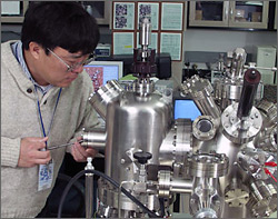
Capability of use with ultra-high vacuum makes NREL Scanning Probe Microscopy particularly valuable for certain applications.
SPM encompasses a group of techniques that use very sharp tips that scan extremely closely (several nm) to or in contact with the material being analyzed. The interaction between the tip and the sample surface is monitored and controlled to generate the output, which defines the SPM technique being used. A large number of interactions can be measured, including force, current, and capacitance. This makes SPM flexible and capable of providing information on different properties of materials.
Main Characteristics of Scanning Probe Microscopy
- High-spatial resolution, reaching atomic resolution in some applications
- Digital data acquisition, allowing real 3D imaging and measurements such as roughness and surface line scan
- Nondestructive
- Capability to analyze samples with a broad range of conductivities (from conductors to insulators), although not by all techniques
- Capability to perform SPM in air or in ultra-high vacuum, as appropriate
- Field of view from atoms up to about 100 µm (vertical limit of about 7 µm)
Scanning Probe Microscopy Techniques
Conductive Atomic Force Microscopy
Scanning Kelvin Probe Microscopy
Scanning Capacitance Microscopy
Contact
Share