Dual-Beam Sample Preparation

NREL uses a dual-beam focused ion-beam (FIB) workstation for ion milling, metal deposition, ion imaging, and electron imaging on the micrometer and nanometer scale of advanced photovoltaic materials and devices.

Materials characterization is an essential strength of the focused-ion beam (FIB) platform. Material can be removed or added while observing the evolution of the surface topography features of the specimen with ion beam stimulated secondary electrons

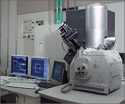
NREL's dual-beam focused-ion beam workstation for fabricating microscopy samples and nanostructures.

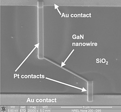
The dual-beam FIB supports other analytical tools such as transmission electron microscopy (TEM), and precise, site-specific sample preparation for TEM, SEM, and local electrode atom probe (LEAP). See below examples. 

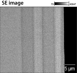
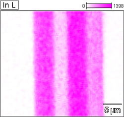
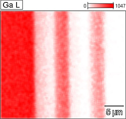
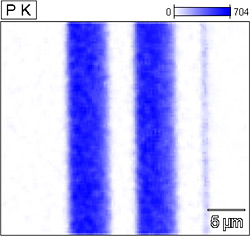
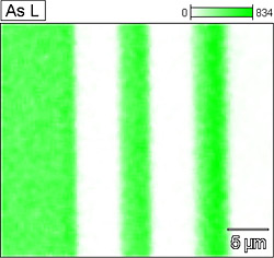
Acquiring chemical spectra and elemental maps is another feature of this system with energy-dispersive spectroscopy (EDS). Three-dimensional chemical reconstructions can be obtained by combining controlled ion milling with chemical mapping. The FIB is equipped with a gas injection system (GIS) platinum metal deposition capability that can be used with either ion-beam-assisted or electron-beam-assisted chemical vapor deposition. Using a digital patterning generator also allows for complete FIB milling or deposition of complex structures with software-supplied parameters or by direct input of bitmap files (or both). See below examples. 

Examples of Dual-Beam Focused-Ion-Beam Sample Fabrication Capabilities


SEM microphoto of contacts attached to a nanowire.

FIB: chemical vapor deposition — SEM image taken in the dual beam FIB showing nano deposition with GIS of Pt contacts to a single GaN nanowire.


First of three TEM images showing cutting of trenches to remove a wafer section and transferring that section to a grid post. This is an overhead view of the cut trenches.
Second of three TEM images showing cutting of trenches to remove a wafer section. This is a side view, showing the depth of the rectangular trenches, with a slim bridge of material in the middle.

Third of three TEM images showing cutting of trenches to remove a wafer section and transferring that section to a grid post. Here the wafer section is lifted out and seen from the side.

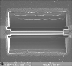
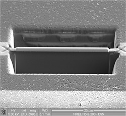
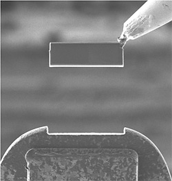
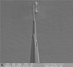
FIB: TEM sample preparation — FIB prepared TEM cross-section (from A to C). Opposing trenches are milled out with the Ga+ ion source and a 1-2 µm thin section is left free standing in the wafer. A side view shows the depth of the trenches. The section is then welded to the micro-manipulator, extracted from the wafer then transferred and welded to a TEM grid post. Final thinning down to a thickness of < 100nm is achieved using low incident angles and low Ga ion current.


SEM image of sharpened probe sample tip.

FIB: LEAP sample preparation — SEM image taken in the dual beam FIB showing sharpened LEAP sample tip prepared by Ga+ ion milling in the FIB


Scanning electron image of cross-section of a multijunction solar cell followed by EDS elemental maps of the indium, gallium, phosphorus, and arsenic in the cross-section.


FIB: EDS elemental mapping — EDS elemental maps taken in the dual beam FIB showing In, Ga, P, and As distributions in cross-section of a III-V compound semiconductor multi-junction solar cell.


Scanning electron image of cross-section of a multijunction solar cell followed by EDS elemental maps of the indium in the cross-section.
Scanning electron image of cross-section of a multijunction solar cell followed by EDS elemental maps of the gallium in the cross-section.

Scanning electron image of cross-section of a multijunction solar cell followed by EDS elemental maps of the phosphorus in the cross-section.
Scanning electron image of cross-section of a multijunction solar cell followed by EDS elemental maps of the arsenic in the cross-section.

Contact


Share