Atomic Force Microscopy
NREL uses atomic force microscopy (AFM) to analyze materials.
How It Works
AFM operates in several modes. In contact mode, a tip that is attached to a cantilever is scanned over the sample surface, while the force between tip and sample is measured.
While the tip is scanned laterally, the force is kept constant by moving the cantilever/tip assembly up and down, so that the deflection of the cantilever is kept constant. The vertical movement of the cantilever/tip assembly is recorded and used to generate an image of the topography of the sample.
For very flat samples, the vertical position of one edge of the cantilever is kept fixed, while the edge with the tip is allowed to move vertically as the sample topography changes. This vertical movement is monitored and used to generate the topographic image.
In another mode, the cantilever is oscillated close to its resonant frequency, while the amplitude of the oscillation is measured. As the cantilever/tip assembly approaches the surface, the interaction changes the resonant frequency, which in turns changes the oscillation amplitude. The change in the amplitude is the interaction that will be probed and generate the image.
In all these modes, the position of the cantilever is measured with the help of a laser, which reflects on the top of the cantilever just above the tip to a set of photodiodes. Because it uses the force as interaction, AFM can generate high magnifications (up to atomic resolution) of almost any type of sample, from insulators to conductors. Because the interaction force is generally small (less than the bonding force between atoms), even soft samples, such as biological materials, can be analyzed.
Several other modes are possible with AFM. For instance, in contact mode, friction between the tip and the sample may twist the cantilever, causing a lateral movement of the laser on the photodiodes, which generates an image in lateral force mode. This is used to distinguish different phases on the sample that have similar topography. Some of the special modes of analysis that we use include conductive AFM, scanning kelvin probe microscopy, and scanning capacitance microscopy.
Capability Examples
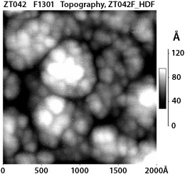
High-resolution AFM image of Zn2SnO4/glass, where grains smaller than 100 Å can be observed.
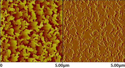
Left: AFM image of a GaP/Si sample. Right: By measuring the cantilever vertical displacement, with the feedback signal on, an image equivalent to the derivative of the AFM image is obtained. This image is particularly useful to detect sudden variations of the topography, such as steps on the top of the terraces.
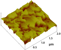
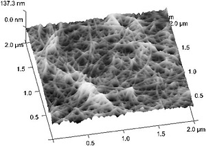
Three dimensional AFM image of a GaP/Si sample. This is a real 3-dimensional representation of the data, which can be rotated to reveal features not observed in a given orientation.
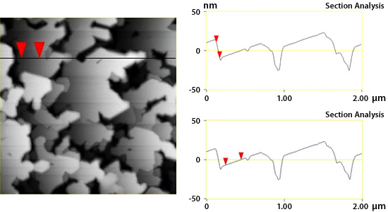
Topography and linescans of a GaP/Si sample. Because of the digital character of AFM data, linescans can be generated from any part of the image, and it is also possible to measure the angle between features. In the present case, the angle between the sections marked by the red arrows is 23.5°.
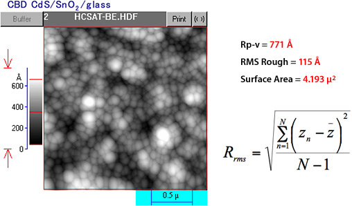
Other parameters that can be automatically obtained from AFM analysis include peak-to-valley distance, roughness and image surface area.
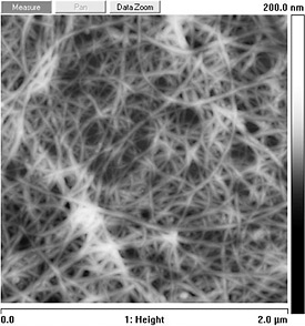
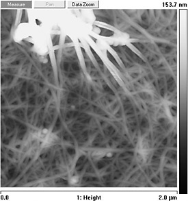
AFM images of carbon nanotubes. The image on the top bottom shows the entanglement of several nanotubes.
Contact
Share