Electron-Beam-Induced Current Measurement
For assessing semiconductor crystal quality, NREL uses scanning electron microscopy to measure electron-beam-induced current (EBIC).
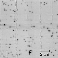
EBIC image of a GaAsP-on-Si solar cell revealing threading dislocations crossing the p-n junction.
In presence of an electrostatic field (p-n junction), electron-hole pairs (e-h) excited by the electron beam can be collected and the resulting current measured with a picoamplifier. EBIC provides information about the location of the junction and estimates of the diffusion length and surface recombination. EBIC mapping reveals grain boundaries and dislocations by their distinct recombination behavior. The dislocation density in semiconductors can be determined with very high precision in the 105–108 cm2 range. EBIC observations can be performed in the JEOL 5800 at temperatures between 15 K and 300 K, which can be used to estimate the activation energy of local traps (up to 0.2–0.3 eV) or identify midgap states.
Share