Materials Characterization
For high-throughput experiments, NLR's materials discovery and design researchers have spatially resolved measurement capabilities, also known as mapping capabilities, and specialized characterization instruments.
These tools are complemented by our large number of single-point, specialized characterization instruments, allowing us to study the most interesting samples in more detail.
Chemical Composition Mapping
Method: X-Ray Fluorescence (XRF)
Instrument: Fisher XDV XRF
Measures: Composition and thickness
Samples: <12" square
Resolution: 0.3-3 mm
Time per point: 3-5 min
Features: Ti lightest element
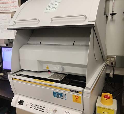
Method: X-Ray Fluorescence (XRF)
Instrument: Fisher XUV XRF
Measures: Composition and thickness
Samples: <6" square
Resolution: 0.3-3 mm
Time per point: 3-5 min
Features: >Al, vacuum
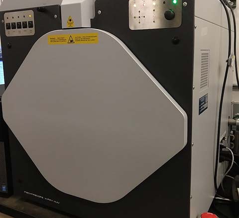
Method: X-Ray Fluorescence (XRF)
Instrument: Bruker Tornado XRF
Measures: Composition and thickness
Samples: <6" square
Resolution: 0.01-3 mm
Time per point: 3-5 min
Features: >Al, vacuum, micro
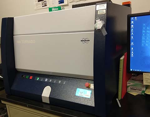
Method: Wavelength dispersive X-ray fluorescence (WD-XRF)
Instrument: Rigaku Primus-IV WD-XRF
Measures: Composition and thickness
Samples: 24 x <2" square
Resolution: ~3 mm
Time per point: ~10 min
Features: C lightest element. Mapping capability. Can measure composition of light anions (e.g., N, O).
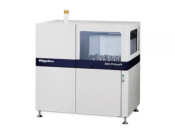
Method: Rutherford Back Scattering (RBS)
Instrument: National Electrostatics Corp RBS
Measures: Composition and thickness
Samples: <2" square
Resolution: 1 mm
Time per point: 30 min
Features: >N, vacuum
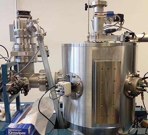
Crystal Structure Mapping
Method: X-Ray Diffraction (XRD)
Instrument: Bruker D8 Discover XRD
Measures: Structure and phase content
Samples: <4" square
Resolution: 1-2 mm
Time per point: 3-5 min
Features: 2D detector
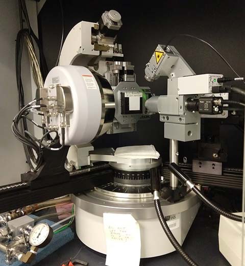
Method: High-Resolution X-Ray Diffraction and Reflectivity (XRD)
Instrument: Rigaku Smartlab
Measures: Epitaxial film crystal structure, orientation, quality, and thickness
Samples: <4" circle
Resolution: 1-2 mm
Time per point: Depends on measurement, typically 60 min per point
Features: 2D detector, high resolution optics, heated stage to 1100 °C.
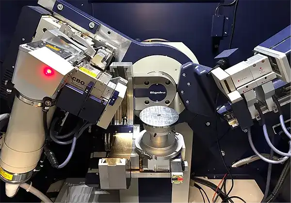
Method: Single Crystal X-Rray Diffraction (SCXRD)
Instrument: Bruker D8 Venture Ga MetalJet
Measures: Single crystal structures, capillaries, thin films, and high pressure experiments in diamond anvil cells
Samples: minimum crystals ~10 microns
Resolution: n/a
Time per point: Depends on measurement, typically 5-10 min per capillary and 20-300 min per single crystals
Features: 2D detector, high resolution optics, and cryostream 80–400K
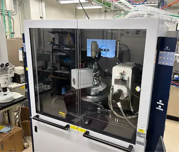
Optical Property Measurements
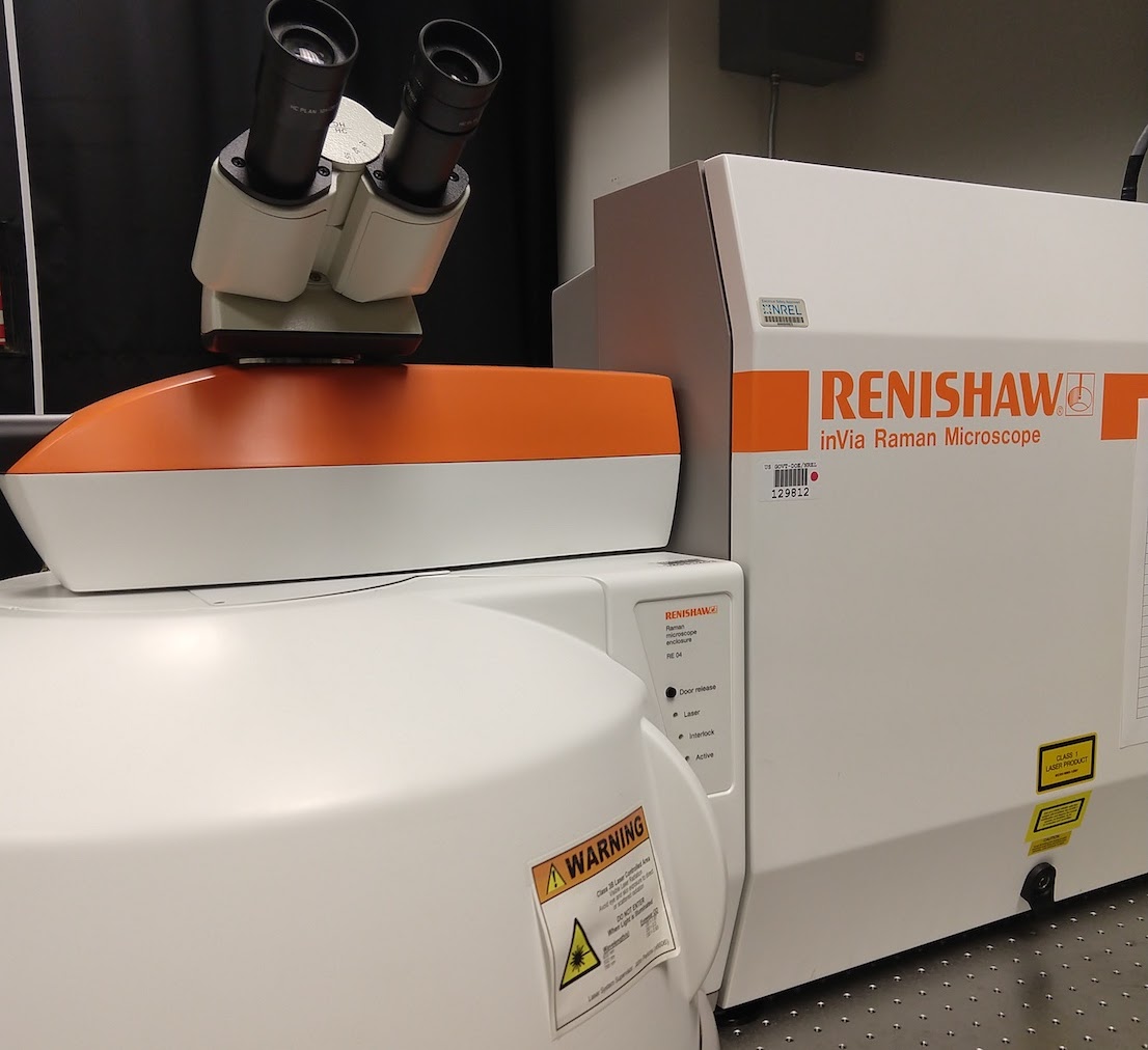
Method: Raman and Photoluminescence
Instrument: Renishaw in Via Raman Microscope
Measures: Vibration modes and phase ID
Samples: <2" square
Resolution: 1 um
Time per point: 5 min
Features: Multiple lasers
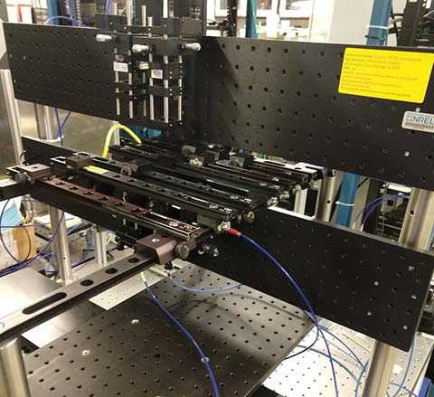
Method: Optical Spectroscopy
Instrument: Custom with Ocean Optics Spectrometer
Measures: Bandgap and absorption coefficient
Samples: <6" square
Resolution: 1 mm
Time per point: 3 sec
Features: Diffuse and specular ultraviolet visible spectroscopy (UV-Vis-NIR)
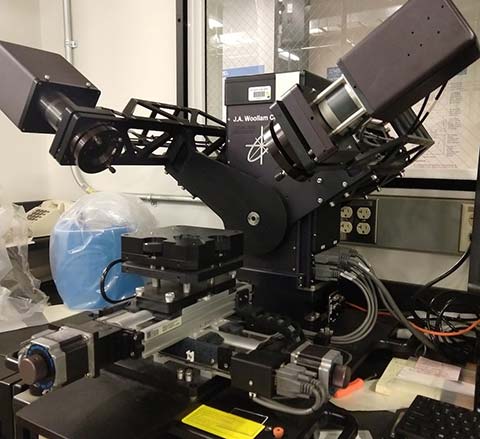
Method: Spectroscopic Ellipsometry
Instrument: J.A. Woollam Ellipsometer
Measures: Thickness and refractive index
Samples: <6" square
Resolution: 1 mm
Time per point: 10 sec
Features: Variable angle and UV-VIS-NIR
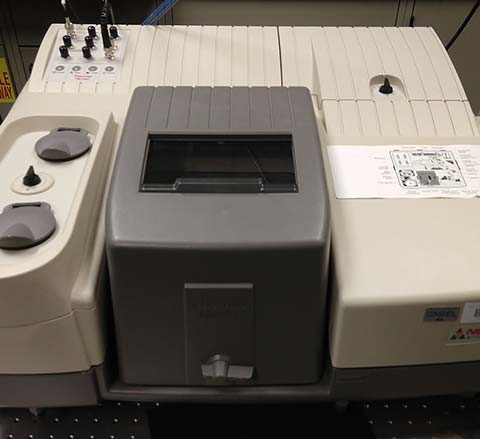
Method: Fourier Transform Infrared Spectroscopy (FTIR)
Instrument: Thermo Scientific FTIR
Measures: Plasmons and vibrations
Samples: <6" square
Resolution: 3 mm
Time per point: 5 sec
Features: 1.8-25 um
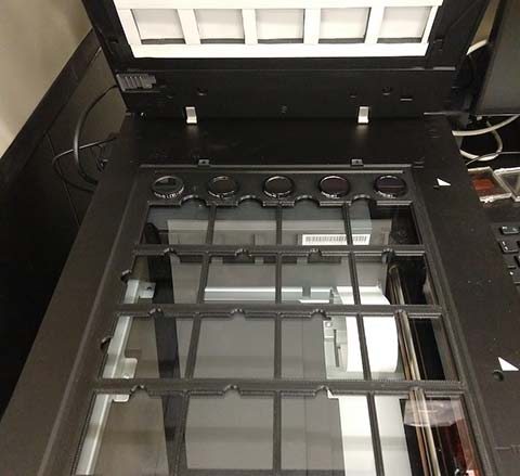
Method: Colorimetry
Instrument: Epson Perfection V850 photo scanner
Measures: Film images and color
Samples: <8" square
Resolution: 1 um
Time per point: <1 sec
Features: Custom holder and software
Electrical Property Measurements
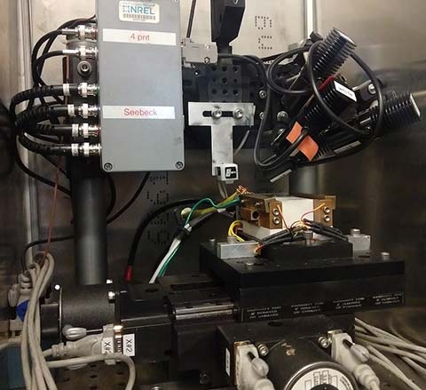
Method: 4-Point Probe
Instrument: Custom 4-point probe
Measures: sheet resistance
Samples: 2" square
Resolution: 3 mm
Time per point: 15 sec
Features: Heaters for measuring Seebeck
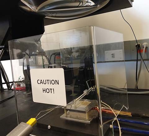
Method: Two-Terminal Measurements
Instrument: Custom JV/CV/IS
Measures: Resistance, capacitance, and impedance
Samples: <6" square
Resolution: 1 mm
Time per point: 5-30 sec
Features: Solar simulator and T/ambient control
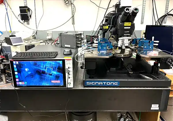
Method: IV-CV Sweeping and Multiterminal Measurements
Instrument: Keithley 4200
Measures: Transistor and capacitor characteristics
Samples: <3" square
Resolution: 1 mm
Time per point: 10 min
Features: Microscope probe station
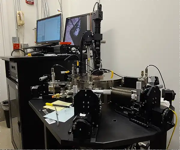
Method: Cryogenic Environment Probing
Instrument: LakeShore 8425 Probing Station
Measures: 2, 3, and 4 terminal electrical measurements, including Hall effect, with in-situ probing
Samples: up to 4 x 1cm square (or similar)
Resolution: NA
Time per point: Depends
Features: 10K–400K sample environment with ≤2 Tesla magnet and up to 6 in-situ probes. Capabilities include gated measurements, fully triaxial shielded cabling, electrometer, picoammeter, and nanovoltmeter for difficult measurements/samples
Magnetic Property Mapping
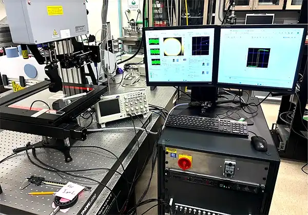
Method: Magneto Optical Kerr effect
Instrument: Durham MagnetoOptics NanoMOKE3 Wafer Mapper effect
Measures: Magnetic hysteresis loops and domain Imaging effect
Samples: <8" round effect
Resolution: <10 μm effect
Time per point: 30 sec effect
Features: Holders and analysis software for full wafer mapping from ambient to ~400°C
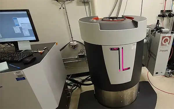
Method: Magnetometry, Heat capacity, Thermal Conductivity, Electrical Transport, and Optical Properties
Instrument: Quantum Design Physical Properties Measurement System
Measures: AC susceptibility and DC magnetization (including under illumination); heat capacity, thermal conductivity, electrical transport (including a rotator), and magneto-PL
Samples: <5mm square
Resolution: NA
Time per point: Depends
Features: 14 Tesla magnet, temperatures from 1.8–400K
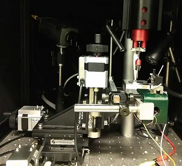
Method: Kelvin Probe measurement
Instrument: KP Technology measurement
Measures: Work function and surface photovoltage measurement
Samples: <6" square measurement
Resolution: 1 mm measurement
Time per point: 10 sec measurement
Features: Variable angle and UV-ViS-NIR
Surface Property Mapping
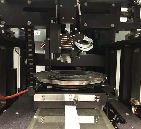
Method: Thickness Profilometry
Instrument: Dektak Profilometer
Measures: Film thickness
Samples: <6" round
Resolution: 1 um
Time per point: 30 sec
Features: Holders and analysis software for full wafer mapping
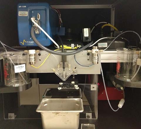
Method: Scanning Droplet Cell (SDC) Mapping
Instrument: Custom SDC instrument
Measures: Cyclic voltammetry and photocurrent
Samples: <2" square
Resolution: 2 mm
Time per point: 30 sec
Features: Corrosion testing and LED-based light
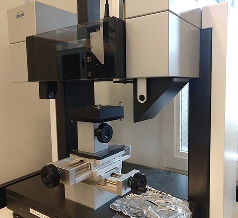
Method: Contact Angle Measurement
Instrument: Kruss-Scientific
Measures: Contact angle
Samples: <6" square
Resolution: 3 mm
Time per point: 15 sec
Features: Custom solutions
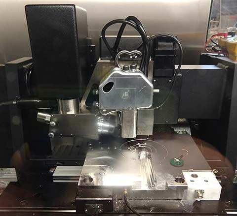
Method: Atomic Force Microscopy (AFM)
Instrument: Bruker AFM
Measures: Root mean square roughness and grain size
Samples: <6" square
Resolution: 1 nm
Time per point: 30 min
Features: Vacuum transfer
Publications
Instrument for Spatially Resolved, Temperature-Dependent Electrochemical Impedance Spectroscopy of Thin Films Under Locally Controlled Atmosphere, Review of Scientific Instruments (2021)
Combinatorial In Situ Photoelectron Spectroscopy Investigation of Sb2Se3/ZnS Heterointerfaces, Adv. Mater. Interfaces (2016)
Development and Application of an Instrument for Spatially Resolved Seebeck Coefficient Measurements, Rev. Sci. Instrum. (2013)
Contacts
Share
Last Updated Dec. 6, 2025
