Scanning Kelvin Probe Microscopy
NREL uses scanning kelvin probe microscopy (SKPM) to measure two-dimensional distributions of contact potential difference (CPD) between the tip and the sample with resolution in the nanometer range.
The CPD can be converted to the work function of the sample if the measurement is performed under thermoequilibrium state; and it is the electrical potential when the sample is illuminated or a bias is applied to the sample.
How It Works
In SKPM, the atomic force microscopy (AFM) system operates in non-contact mode, and a conductive tip is oscillated at the first resonant frequency of the cantilever over the sample surface as it is scanned laterally. The topographic data is taken by controlling the atomic force between the tip and sample. In addition to the atomic force, a long-range electrostatic force also exists between the tip and sample, which is determined by the CPD between them. The electrostatic force is detected by applying an ac voltage to the tip and using a lock-in amplifier. The ac voltage frequency is set at either the second resonant frequency of the cantilever or a low frequency (~20 kHz) that is far off the first resonant frequency, in order to avoid the interaction between the topographic and electrical signals. The electrostatic force is zero when the CPD is completely compensated by a dc voltage applied to the tip. In this case, the CPD is equal to the applied dc voltage.
In our laboratory, we have SKPM capability both in air and in UHV. SKPM measurement on solar cell cross-sections help to identify and assess p-n junctions, while SKPM performed on the surface of semiconductors allows the investigation of local electrical potential and band bending distribution.
Examples of Scanning Kelvin Probe Microscopy Capabilities
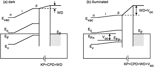
Schematics of band diagrams of the tip and sample in SKPM measurement. Kelvin probe measures the work function difference between the tip and the sample when in thermoequilibrium state (a), and measures the electrical potential when the sample is illuminated (b), which is the sum of the difference in workfunction and internal/external-applied voltages.
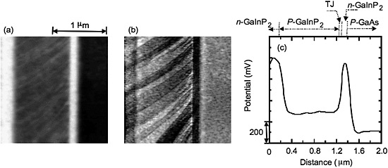
(a) SKPM potential and (b) corresponding AFM topographic images from the cross-section of a GaInP2/GaAs tandem-junction solar cell. (c) Averaged potential profile along the vertical direction in (a), showing the potential at the top, tunneling, and bottom junctions.
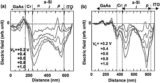
Distributions of the electric field in a-Si:H n-i-p solar cells with (a) and without (b) buffer layers between the n and i and i and p layers. The electric field is deduced by taking the first derivative of the SKPM potential measurement. It is clear from the data that the incorporation of buffer layers improved the electric field distribution.
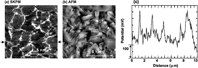
(a) Electrical potential measured by SKPM and (b) corresponding AFM topographic image from Cu(In,Ga)Se2 thin films. The SKPM data shows a higher electrical potential or an upward band bending at grain boundaries. (c) Line profile along the arrows in (a).
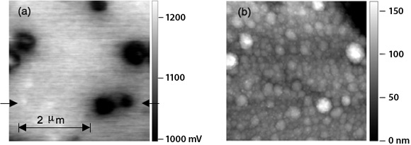
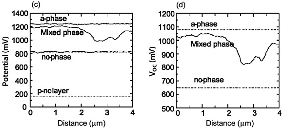
(a) SKPM potential and (b) AFM topographic images taken on the p-layer of a-Si:H and nanocrystalline (nc-Si:H) mixed-phase n-i-p device, showing that the nc-Si:H phase aggregate to clusters in size of ~500 nm. From the measured potential values shown in Fig. (c), local Voc distribution on the mixed-phase device was deduced as shown in Fig. (d).
Contact
Share