Transmission Electron Microscopy
NREL uses transmission electron microscopy to probe properties of thin foils such as in chemistry, microstructure, and crystalline defects.
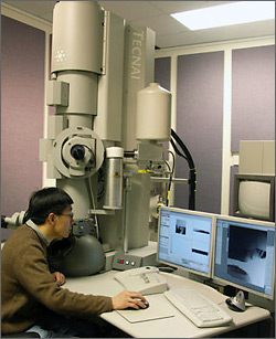
F-20 UT Transmission Electron Microscope.
In the conventional TEM mode, the condenser lenses of the microscope are adjusted to illuminate the sample with a parallel coherent beam of electrons, usually several μm across.
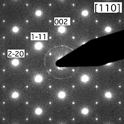
Selected area transmission electron diffraction pattern showing 1/2{111} superlattice spots arising from strong atomic ordering of As and Sb atoms on {111} planes in molecular-beam-epitaxy grown GaAsSb.
Electron Diffraction
To view the diffraction pattern from a sample, the imaging-system lenses of the microscope are adjusted such that the back focal plane of the objective lens acts as the object plane for the intermediate lens. This causes the diffraction pattern to be projected onto the viewing screen. Selected area transmission electron diffraction patterns can be obtained from localized regions of the sample by inserting a selected area diffraction aperture into the image plane of the objective lens. Diffraction patterns from small areas can also be obtained by converging the beam producing a convergent beam diffraction pattern, but this destroys any coherence and broadens the diffraction spots into discs. Selected area diffraction can be used to determine whether a specimen is single crystal, polycrystalline, or amorphous; identify the crystallographic structure, symmetry, and orientation of samples; measure the lattice parameter; identify if more than one phase is present, etc. Convergent beam electron diffraction allows diffraction patterns to be obtained from very small areas. It can be used to measure specimen thickness and lattice parameters, and to determine point group and space group information.
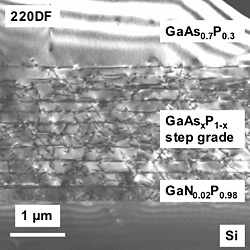
Diffraction contrast cross-sectional TEM dark-field image reveals misfit dislocations generated in GaAsxP1-x compositionally step graded layers grown by metal organic chemical vapor deposition on Si.
Amplitude-Contrast Imaging
Amplitude-contrast images are formed by inserting an "objective" aperture into the back focal plane of the objective lens that blocks most of the diffraction pattern that lies outside of the aperture. Bright-field images are formed, if we use a small objective aperture to select only the directly transmitted beam of electrons. Dark-field images are formed, if we use the objective aperture to select electrons that have been scattered by the sample. In crystalline materials, diffraction contrast arises from coherent elastic scattering of electrons at special, Bragg angles. For good diffraction contrast, the sample is normally tilted such that only one diffracted beam is excited. This is referred to as a two-beam condition. In dark-field images, areas that appear bright correspond to areas where the atomic planes corresponding to the selected diffracted beam are locally in the Bragg condition.
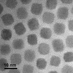
High-resolution TEM image of array of colloidal PbTe nanocrystals synthesized to study multiple exciton generation in semiconductor nanocrystals.
Diffraction Contrast Imaging
Diffraction contrast imaging is particularly useful in studying the nature of defects in crystals. In quite a few materials (such as AlGaAs), the structure factor of some diffracted beams is sensitive to the difference in atomic scattering factors of the constituents. Dark-field imaging with such diffracted beams can reveal compositional changes in samples. Mass-thickness contrast arises because areas of higher atomic number (Z) or greater thickness scatter electrons more strongly thereby appearing dark in bright-field images and bright in dark-field images. It is particularly useful for imaging non-crystalline materials (such as polymers) and biological samples.
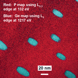
Energy-filtered TEM elemental map obtained using Gatan image filter reveals Ge nanowires embedded in GaInP matrix
Phase-Contrast Imaging
Phase contrast occurs whenever more than one beam contributes to the image, and we see fringes. It arises from the difference in phase of the electron waves that occurs when they are scattered while passing through a thin sample. Examples of phase contrast include moiré patterns; Fresnel contrast at defects; and high-resolution TEM (HRTEM) imaging. Phase-contrast images can be difficult to interpret since the contrast is sensitive to many factors including sample thickness, orientation, and scattering factor and changes in the astigmatism and focus of the objective lens. In HRTEM imaging, a large diameter objective aperture is used to select multiple beams to form an image containing lattice fringes that can reveal information about the atomic structure of the sample. The lattice fringes are not direct images of the atomic structure but can give information on the lattice spacing and atomic structure of the crystal. Full interpretation of the images, e.g., of the atomic structure of defects and interfaces, requires extensive computer simulation, because when an experimental image is recorded one loses phase information, and this means one cannot directly infer the atomic structure from the image.
High-resolution TEM image of array of colloidal PbTe nanocrystals synthesized to study multiple exciton generation in semiconductor nanocrystals.
Energy-Filtered Imaging and Diffraction Using GIF on F20 UT
In this mode, TEM images or diffraction patterns are formed using the intensity selected from part of the electron energy loss spectroscopy (EELS) spectrum using the GIF. Energy-filtered imaging with the GIF enables elemental mapping in the TEM mode to a high spatial resolution. Energy-filtered electron diffraction patterns allows observation of fine details not possible in unfiltered images.
Contact
Share