Scanning Transmission Electron Microscopy
In the scanning transmission electron microscopy (STEM) mode, NREL adjusts the microscope lenses to create a focused convergent electron beam or probe at the sample surface.
This focused probe is then scanned across the sample and various signals are collected point-by-point to form an image. The convergence of the beam destroys its coherency.
Atomic Resolution Z-Contrast Imaging
Z-contrast images are formed by mapping the intensity of high-angle scattered electrons as the electron probe is scanned across the specimen. Z-contrast images are incoherent, have double the resolution of coherent images, and do not reverse contrast with focus or specimen thickness. The images represent a direct map of the scattering power at atomic resolution. There is no phase problem in an incoherent image, so it can be directly inverted to the object, avoiding the need for numerous simulations of trial structures. Because the image is formed from high-angle scattering from the atomic nuclei, the scattering cross section depends on atomic number (Z) squared. The F20 UT provides directly interpretable, chemical sensitive, and high-resolution (~0.14nm) STEM Z-contrast images.
Elemental mapping using energy dispersive X-ray spectroscopy (EDS) and electron energy loss spectroscopy (EELS). High special resolution compositional maps and line profiles may be obtained in the STEM mode by collecting the EDS and EELS signals point-by-point as one scans the electron probe across the sample. In the F20 UT, using the Z-contrast image to locate the probe over specific atomic columns, EELS and EDS may be performed to give composition and electronic structure information at atomic resolution.
Scanning Transmission Electron Microscopy Capability Examples
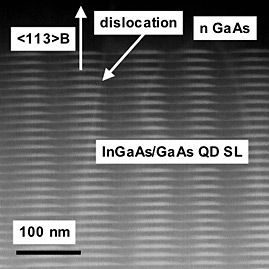
STEM Z-contrast cross-section image of metal-organic-chemical-vapor-deposition grown InGaAs/GaAs quantum dot superlattice solar cell showing fairly regular vertical columns of quantum dots.
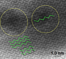
Atomic-resolution STEM Z-contrast imaging shows the details of the void-like defects in In2O3 thin films.
Oxygen vacancy clusters in In2O3
Z-contrast image
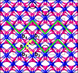
Atomic structure
Atomic-resolution Z-contrast image reveals nanodomains in CIGS thin films.
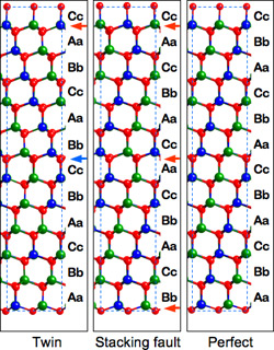
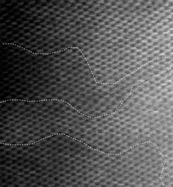
Atomic structure of twin boundaries in CIGS thin films as shown by STEM Z-contrast imaging.
Contact
Share