Scanning Tunneling Microscopy
NREL uses scanning tunneling microscopy (STM) to measure the tunneling current between a conductive tip and the sample surface when a potential is applied between them.
It is the first developed scanning probe microscopy technique.
How It Works
The current, in the range of 10 pA to 100 nA, is monitored by an electric circuit. A feedback circuit keeps the tunneling current constant, by adjusting the distance of the tip from the surface. By measuring the vertical position of the tip at each point, an image of the sample surface is generated (topographic image). For very flat samples, the vertical position of the tip may be kept constant, and the image is formed by the variation of the current.
Other methods of data acquisition are also possible, such as measuring local variations of the tunneling current as the voltage or the tip-surface distance are varied. These measurements are called scanning tunneling spectroscopy (STS). Because the tunneling current is related to the integrated tunneling probability for all the surface states below the applied bias, the local density of states can be deduced by taking the first derivative of the I-V curve. If I-V curves are taken at every pixel of the image, a spatial mapping of a specific surface state can also be obtained. Also, local values of the work function can be obtained from I-Z curves, which are generated by sweeping the tip-sample distance (Z) while acquiring the tunneling current (I).
Because STM is based on measuring the current between the tip and the sample, STM can only analyze conductor and semiconductor samples. Also, because most of the current is generated between the most outward atoms of the tip and the surface, atomic images can be generated only for atomically flat samples. Most atomic work requires the analysis to be done under ultra-high vacuum, to avoid surface contamination from exposure to the atmosphere.
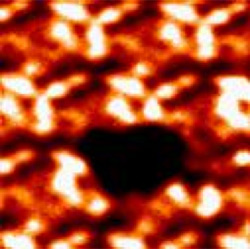
Scanning Tunneling Microscopy Capability Examples
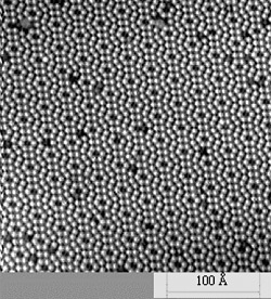
2D STM image of Si(111) 7×7 Reconstruction
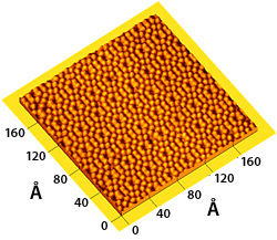
3D STM image of Si(111) 7×7 Reconstruction
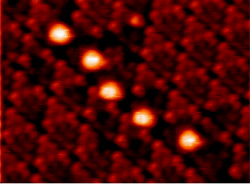
Occupied-state STM image taken on a Si(111)7×7 surface, showing two 7×7 domains and the faulty domain boundary between them. The small Si clusters are preferably located at grain boundaries.
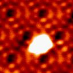
Unoccupied-state image showing a Si cluster on the Si(111)7×7 surface (left), and the current image (below-left) extracted from the STS spectra (I-V) taken at every pixel and at a tip voltage of -1 V, showing the two-dimensional mapping of the local density of state at 1 eV above the Fermi level.
Contact
Share