X-Ray and Energy-Loss Spectroscopy
NREL’s x-ray and energy-loss spectroscopy techniques form the basis of analytical microscopy and enable qualitative and quantitative compositional analyses, elemental mapping, and electronic property analysis for a variety of elements.
How It Works
The signals used in energy dispersive X-ray spectroscopy (EDS) and electron energy-loss spectroscopy (EELS) are caused by inelastic scattering (involves loss of energy) of electrons as they pass through the sample.
The field emission gun of the F20 UT scanning transmission electron microscope allows analyses to be performed on a nanometer, and, in some cases, on an atomic scale. The characteristic X-rays typically used in EDS are created when high-energy electrons of the beam eject inner shell electrons from atoms in the sample, and the ionized atoms return to their lowest energy states by replacing the missing inner shell electrons by electrons from the outer shells. This process results in either the emission of an X-ray or an Auger electron, whose energy of emission is characteristic of the difference in energy of the two electron shells involved, thereby providing a unique signature to identify the type of atoms present. In an EDS spectrum, we see sharp peaks corresponding to the characteristic X-rays emitted by the atoms of the different elements present in the sample.
EELS looks at the energy distribution of the electrons that have been inelastically scattered while passing through the sample. Low energy losses (< 50 eV) correspond typically to electrons that have interacted with the weakly bound outer-shell electrons of the atoms in the sample and provide information about the electronic properties of the material. High losses (> 50 eV) correspond to electrons that have been inelastically scattered by the inner electron shells and so contain information characteristic of the atoms in the sample. A typical EELS spectrum contains both a series of peaks at low energies created by plasmon oscillations or other phenomena and a series of low intensity ionization edges at high-energy losses, whose onset position is characteristic of the different types of atoms in the sample. The fine structure of the ionization edges can provide information on chemical bonding and atomic configurations.
Electron Energy-Loss Spectroscopy Capability Examples
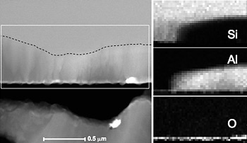
Scanning transmission electron microscopy (STEM) EDS mapping reveals the chemical distribution at the back contact in a Si solar cell.
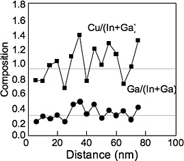
STEM EDS line profile reveals chemical fluctuation in CIGS. EDS data taken from the large box gives the averaged chemical composition, which is consistent with other measurements.
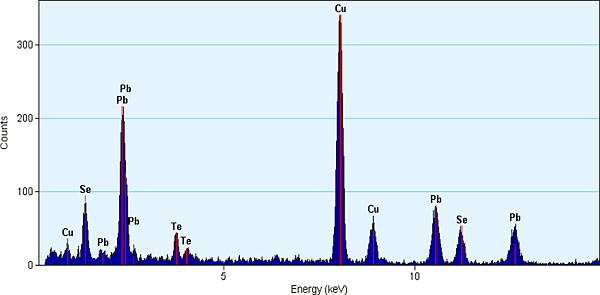
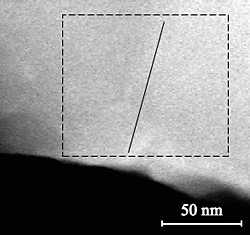
TEM EDS reveals a mixture of PbSe and PbTe nanoparticles present on carbon support film Cu grid.
Energy Dispersive X-Ray Spectroscopy Capability Examples
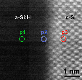
High-resolution Z-contrast image of a c-Si/a-Si interface from a high-efficiency Si heterojunction solar cell. The image reveals an atomically abrupt and flat c-Si/a-Si interface (see next).
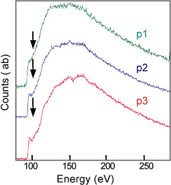
Electron energy-loss spectroscopy of the same interface at three different positions reveals changes in electronic properties from the c-Si to the interface and to the a-Si regions (see peaks indicated by black arrows).
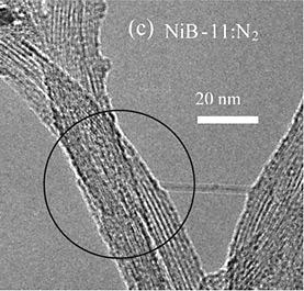
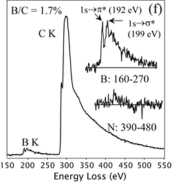
EELS demonstrates that boron has been incorporated into carbon nanotubes.
Contact
Share
