Scanning Capacitance Microscopy
NREL uses scanning capacitance microscopy (SCM) to provide qualitative information on the doping of semiconductor materials using an atomic force microscope.
How It Works
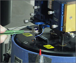
The atomic force microscope features an ultra-high-frequency resonant capacitance sensor connected to a grounded tip via a transmission line attached to a UHF capacitance sensor.
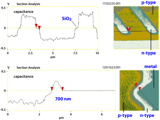
Right: SCM images of Si devices, showing the capability of the technique to distinguish areas with p- and n-type doping. Left: Linescan of the marked locations on the SCM images.
In SCM, the atomic force microscopy tip is scanned in contact mode and, simultaneously with a topographic image, the lateral variations of the capacitance of the sample generate a capacitance image.
Simply speaking, the tip forms one of the electrodes, the semiconductor forms the other electrode, and the oxide on the sample surface is the dielectric. The capacitance signal is a function of the contact area between the tip and the oxide, the properties of the oxide, and the type and concentration of the charge carriers inside the semiconductor.
Sample preparation is very important in SCM, and a polishing procedure for the sample, and a stage where the surface oxide is formed and passivated are in general required for the generation of high-quality and reliable data. For a flat sample, with a good quality and uniform oxide, the capacitance signal will be exclusively controlled by the doping of the material. In SCM, dc and ac bias are applied between the sample and the tip, and the output is the dC/dV signal. The derivative of the capacitance-voltage curve has different signs for p- and n-type semiconductors, which allows the determination of the type of the material being measured. Also, because the degree of depletion of a semiconductor subject to a voltage depends on the doping, regions with higher carrier concentration provide a smaller dC/dV signal than regions with lower carrier concentration. In general, SCM is used to provide qualitative information on doping of semiconductors. With the help of modeling, quantitative analysis is also possible.
Contact
Share
