Conductive Atomic Force Microscopy
NREL uses conductive atomic force microscopy (C-AFM) to analyze materials.
How It Works
C-AFM is a mode of atomic force microscopy in which a conductive tip is scanned in contact with the sample surface, while a voltage is applied between the tip and the sample, generating a current image.
At the same time, a topographic image is also generated. Both, the current and the topographic images are taken from the same area of the sample, which allows the identification of features on the surface conducting more or less current. An electric circuit, with current amplifiers and filters, monitors the current, which can vary from a few pA up to 500 nA.
After acquiring a topographic image, the tip may be moved to a specific desired location. The voltage is then ramped while the current is measured to generate local current versus voltage (I-V) curves.
Several kinds of conductive tips can be used in C-AFM, but the most successful are the conductive diamond-coated silicon tips. Besides having a good conductivity, the diamond layer is resistant to wear. The main advantage of C-AFM over standard electrical measurement techniques is the high spatial resolution. For example, C-AFM measurements on polycrystalline thin films have been able to identify differences in the conductivity between grain boundaries and the interior of the grains. Also, C-AFM has been shown to be suitable to identify conducting paths in solar cells and to locate microshunts.
Examples of Conductive Atomic Force Microscopy Capabilities
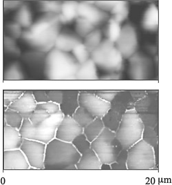
AFM (top) and C-AFM (bottom) images of a CdTe/CdS/SnO2/glass sample after bromine/methanol etch. One electric contact is placed on the SnO2 while the other contact is provided by the tip in contact with the CdTe. Bright regions means higher current. Notice the enhanced conductivity at grain boundaries.
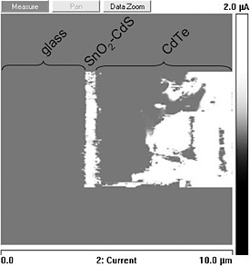
AFM (top) and C-AFM (bottom) images of the cross section of a CdTe/CdS/SnO2/glass device after nitric/phosphoric acids etch and deposition of Au/Cu contact. Notice the short circuit of the device at the bottom of the C-AFM image.
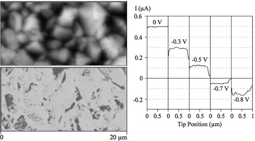
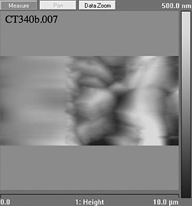
Left: Topographic (top) and current (bottom) images from a CdTe/CdS sample after NP
etch. The NP etch creates a conductive layer over the whole surface of the CdTe film.
Right: Linescans of the current taken over the NP-etched CdTe surface under illumination
and at different forward voltages. Each linescan was taken at the same location and
has a length of 1 µm. The illumination produces a photocurrent that is annulled by
a forward bias equal to 0.64 V, which is the Voc for the device.
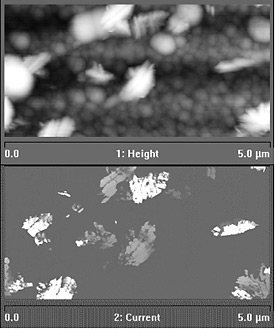
AFM (top) and C-AFM (bottom) images of Si/SnO2/glass. The Si film is composed by an amorphous matrix with some crystalline phase. Because of its higher electric conductivity, the crystalline phase is readily distinguished from the amorphous phase in the C-AFM image.
Contact
Share
