Cathodoluminescence
NREL uses cathodoluminescence (CL) to investigate the distribution of recombination centers in semiconductors including extended defects such as dislocations and grain boundaries, stress fields, compositional fluctuations, and other important features.
How It Works
CL is photon emission stimulated by an electron beam. It has enabled imaging of the electronic and optical properties of semiconductor structures with an ultimate resolution of about 20 nm.
Both spectroscopy and imaging modes are accessible to most CL instruments. In spectroscopy mode, a spectrum of the emitted light is obtained over a selected area under observation in the electron microscope. In imaging mode, a map of the photon intensity (energy resolved with a spectrograph) is acquired instead.
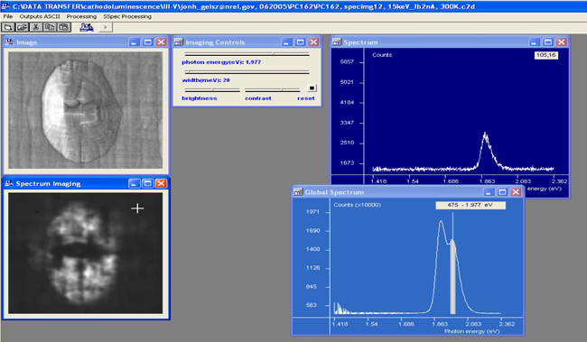
Because these modes cannot be operated simultaneously, information is inevitably lost. At NREL, we have combined spectroscopy and imaging in one single mode: spectrum imaging. In simple terms, spectrum imaging acquires a spectrum for each pixel on the image. This is achieved by synchronizing the scanning of the electron beam with the spectrum acquisition by a multichannel photodetector. In our setup, we can select a silicon CCD or an InGaAs photodetector array, depending on the wavelength of interest (180 nm to 1800 nm). These cryo-cooled detectors offer high sensitivity and superior performance. Our approach to synchronization, based on linescan control, allows acquisition times of 10-20 ms per pixel. For a 125×125 pixel image, the time to acquire the entire spectrum series is about five minutes. When the acquisition is completed, a spectrum-imaging file is generated. The software developed for spectrum imaging (C2DIMAG) processes the spectrum series to reconstruct images of the photon emission (energy resolved) or to extract the spectrum from a selected area. C2DIMAG provides more advanced processing capabilities such as:
- Mapping of the photon energy and full-width-half maximum of selected transitions
- ASCII output
- Quantitative-imaging mode
- Pixel-to-pixel correlation
- Spectrum linescan
- Spectrum fitting routines.
Cathodoluminescence Capability Examples
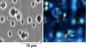
(Left) Faceted pits found in the epitaxy of GaAsP on Si. (Right) Color imaging from the cathodoluminescence emission, revealing the redshift of the spectrum over the facets.
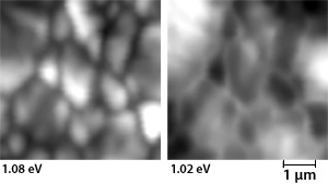
Photon intensity maps for different transitions identified on the emission spectrum of CIGS thin films. Grain boundaries show a distinct electronic behavior.
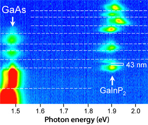
Cathodoluminescence spectrum linescan across a GaInP2/GaAs heterostructure. It shows a resolution better than 43 nm @2keV.
Share
