Materials Discovery Across Technological Readiness Levels
NREL can work across at each technology readiness level—basic science, applied research, and device development—demonstrating competence in a broad range of materials discovery problems.
Basic Science
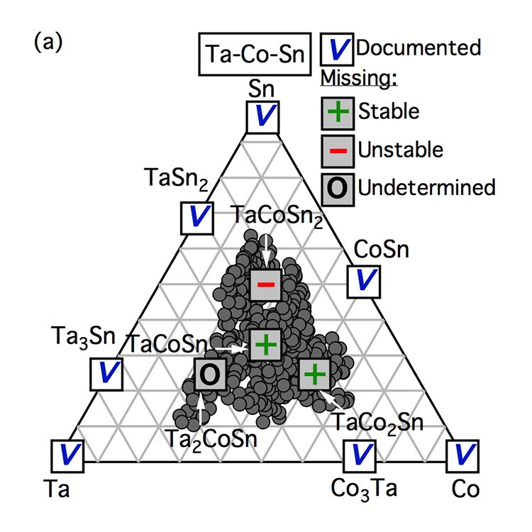
The Materials Discovery process at the most fundamental levels starts from the growth of materials that have never been synthesized before. This includes determining the chemical composition and crystallographic structure of the new materials, and it is akin to discovering a new planet in astronomy or documenting a new species in biology.
Examples of Work
These publications provide examples of our prior work in the basic science area.
Novel Phase Diagram Behavior and Materials Design in Heterostructural Semiconductor Alloys, Science Advances (2017)
Synthesis of a Mixed-Valent Tin Nitride and Considerations of Its Possible Crystal Structures, J. Chem. Phys. (2016)
Theoretical Prediction and Experimental Realization of New Stable Inorganic Materials Using Inverse Design Approach, J. Am. Chem. Soc. (2013)
Applied Research
The more practical aspect of Materials Discovery focuses on materials properties (e.g., optical absorption, electrical conductivity, work function) and the combination of them (e.g., transparent conductors, solar absorbers), rather than on the materials themselves (composition and structure discussed above). Such applied research is the first step toward the material's practical use in devices.
Examples of Work
One aspect of applied research in materials discovery is demonstrating a useful combination of properties in a material that has been previously reported, yet not characterized for these properties. These publications provide examples of our capabilities in this area.
Synthesis and Characterization of (Sn,Zn)O Alloys, Chemistry of Materials (2016)
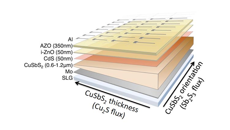
Self-Regulated Growth and Tunable Properties of CuSbS2 Solar Absorbers, Solar Energy Materials and Solar Cells (2015)
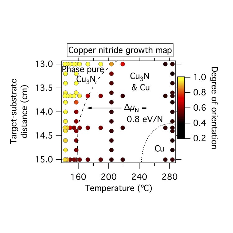
Thin Film Synthesis and Properties of Copper Nitride, a Metastable Semiconductor, Mater. Horiz. (2014)
Another aspect of applied research in materials discovery includes explaining the origins of enhanced/suppressed properties in prototypical functional materials. This allows the distilling of design principles on which the discovery of new materials can be based. These publications provide examples of our research within this area.
Effects of Hydrogen on Acceptor Activation in Ternary Nitride Semiconductors, Advanced Electronic Materials (2017)
Defect Tolerant Semiconductors for Solar Energy Conversion, J. Phys. Chem. Lett. (2014)
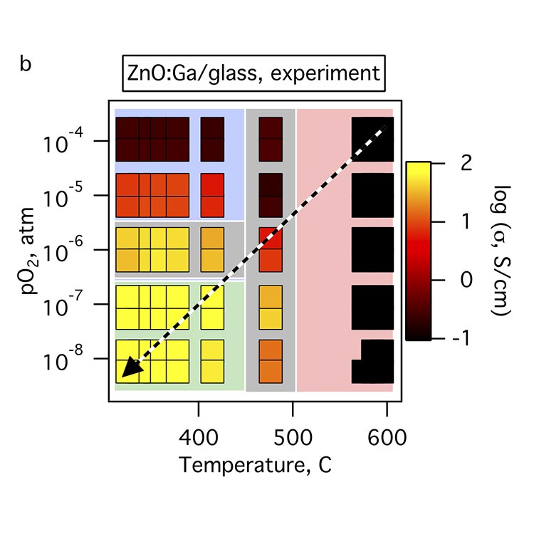
Non-Equilibrium Origin of High Electrical Conductivity in Gallium Zinc Oxide Thin Films, Appl. Phys. Lett. (2013)
Device Development
The ultimate goal of materials discovery is the practical application of new materials in useful devices such as solar cells or transistors. And there are a myriad of interesting challenges that arise from materials interactions, associated with integrating multiple materials with optimal properties into a single device.
Examples of Work
These publications provide examples of our research capabilities in the device development area.
Trade-Offs in Thin Film Solar Cells with Layered Chalcostibite Photovoltaic Absorbers, Advanced Energy Materials (2017)
Combinatorial In Situ Photoelectron Spectroscopy Investigation of Sb2Se3/ZnS Heterointerfaces, Adv. Mater. Interfaces (2016)
Combinatorial Reactive Sputtering of In2S3 as an Alternative Contact Layer for Thin Film Solar Cells, ACS Applied Materials & Interfaces (2016)
Contact

Share
