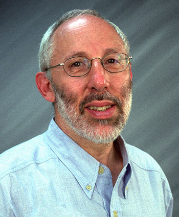
David Ginley
Chief Scientist
David.Ginley@nrel.gov
303-384-6573
 https://orcid.org/0000-0001-5540-3294
David S. Ginley's current activities are in the areas of the general class of defective transition metal oxides including high temperature superconductors, LiTMO2 rechargeable Li battery materials, ferroelectric materials, transparent conducting oxides and electrochromic materials. Another focus of his work is on the development of new nanomaterials for organic electronics and as biofilters etc.
Dr. Ginley's work is directed primarily at the development of new atmospheric processing approaches to photovoltaics.
Some of Dr. Ginley's work in progress is on the development of high quality materials (single crystal films) by pulsed laser deposition, sputtering, IBAD, and characterization of the materials in the doped and undoped states by optical and transport measurements. In addition to developing a fundamental understanding of the interrelationship of structure and electronic properties, Dr. Ginley and his research group are applying what they learn to improved devices, i.e. batteries, frequency agile electronics, photovoltaics, electrochromics and flat panel displays. To transition these results to more practical approaches, they are investigating the development of nonvacuum, direct writeable electronic materials. This is done through the development of nanoparticulate and ink based precursors. This involves the synthesis of the nanoparticles, development of inks and ink deposition techniques, derivation of a fundamental understanding of the sintering behavior of nanoparticles and the evolution of the bulk structural and electronic properties.
Dr. Ginley's work has developed new inks for metallization and the development of highly anisotropic oxide nanoparticles. Currently, Dr. Ginley is also the principal investigator (PI) on new programs in the areas of combinatorial materials science for high throughput discovery of new electrooptical materials including transparent conducing oxides, nitrites and borides.
The approach is also being applied directly to device optimization in aSi. Dr. Ginley's group also initiated a new program in polymer based photovoltaics and other optoelectronic devices especially focusing on the area of interfacial effects and organic/ inorganic structures.
Education
- Ph.D., MIT (Inorganic Chemistry)
- B.S., Colorado School of Mines (Mineral Engineering Chemistry)
Professional Experience
- National Renewable Energy Laboratory Research Fellow/Group Manager
- National Renewable Energy Laboratory Principal Scientist and Group Manager
- Group Manager/Principal Scientist Process Development and Advanced Concepts National Center for Photovoltaics. This group is responsible for developing and implementing new PV process and device technologies. It consists of engineering and advanced concepts teams.
- Team leader for advanced oxides programs including development of materials, theory and devices for new communications technology optical and battery materials.
- Team leader for the advanced projects team for photovoltaic materials and devices. PI for the HTS conductor development program. Involved in development of advanced materials for photovoltaics and batteries.
- Team leader for the 3 million dollar internal research and development (FIRST program) and team leader for the PV and EM Center Business Development Team
- Photovoltaic Devices Branch Manager Managed solid state devices group concentrating on the development of thin film photovoltaics, thermophotovoltaics and crystalline (compound semiconductor and silicon) device processing and characterization. Principal investigator for NREL HTS program. Individual research in pulsed laser deposition of electroactive materials, the development of nanoparticle precursors for electronic materials and investigation of novel etch technologies for electronic materials.
- Sandia National Laboratories Department Manager. Manager of Advanced Materials and Devices Department Department is directed toward the fundamental and applied studies of advanced materials and device development in the semiconductor and superconductor materials areas.
- Sandia National Laboratories Division Supervisor. Supervisor of Solid State Materials Division Division responsible for advanced electronic materials, sensor and device development in a wide variety of materials systems including semiconductors, oxides, superconductors, ionic conductors and battery materials.
- Sandia National Laboratories Senior Member of Technical Staff. Research and development in the areas of photoelectrochemical cells, polycrystalline solar cells, conductive polymers, semiconductor growth and processing, and advanced sensors.
- Sandia National Laboratories Special Assignments. ES&H Directorate 1100 Coordinator (120 people), VP Self Assessment Team Leader (1000 people), Sandia Wide Database Development Group, Sandia Wide NEPA Implementation Comm. Integrated Materials Research Laboratory development team coordinator.
Associations and Accreditations/Memberships
- American Chemical Society (ACS)
- Electrochemical Society (ECS)
- Institute of Electrical and Electronics Engineers (IEEE)
- American Association for the Advancement of Science (AAAS)
- International Society for Optical Engineering (SPIE)
- American Physical Society (APS)
- Materials Research Society (MRS), Area EditorJMR (10/98–Current)
- Board of Directors (Treasurer)
- Fall Meeting Chair (2005)
- President (2010)
- Organizes numerous symposia and workshops on Electronic Communication, Meetings and Education Subcommittees.
- ECS Society Fellow
- Divisional Editor (3/82–10/91)
- Chairman Energy Technology Division (5/88–5/90)
- ASME Member, Associate Editor JSEE
- NREL-related community activities
- Junior Solar Sprint Chief Official, Colorado Science Bowl Chief Judge, Solar Bike Race, Educational Outreach
Patents
- Currently has over 30 patents (15 since at NREL) and over 360 publications in technical journals
- Currently Chief Editor along with David Cardwell (Cambridge University) of the Institute of Physics Handbook of Superconducting Materials. Also working on 3 invited Chapters in oxide electronics and batteries.
Publications
Awards and Honors
- U.S. Department of Energy Outstanding Innovations Award (2007)
- NREL Hubbard Award (2004)
- R&D 100 Award Alumina Nanofibers (2002)
- Federal Laboratory Technology Transfer Award (2002)
- R&D 100 Award Darwin–Electronically Scanning Antenna (2001)
- Fellow of the Electrochemical Society (2000)
- R&D 100 Award (Electroexploded Nanoparticles 2000)
- R&D 100 Award (New Etch Technology 1993) and Federal Laboratory Consortium Tech. Transfer Award (New Etch Technology 1994)
- Sandia: BES Materials Science Award for Outstanding Development with Energy Implications
- Federal Laboratory Consortium Tech. Transfer Award (Hydrogen Passivation of Si Solar Cells)
Share

