Better Explanation of Coalescence-Related Defects Garners Journal Spotlight

New paper aids researchers in understanding defects in coalescing materials, helping to develop low-cost substrates for solar cells.
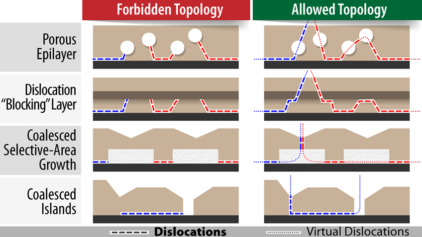
When materials science researchers grow large crystal films, they need to be aware of how dislocations can form in the crystals. A new paper from NREL presents various examples and ways of thinking about these dislocations, some of which are shown here.
A report published by researchers at the National Renewable Energy Laboratory (NREL), Yale University, and the Colorado School of Mines offers a new explanation of a tricky phenomenon—dislocations in coalescing crystalline materials—that was selected for a special highlight by the journal APL Materials.
The paper, titled “Perspective: Fundamentals of Coalescence-Related Dislocations, Applied to Selective-Area Growth and Other Epitaxial Films,” was published in APL Materials. Because of the paper’s broad applicability to the semiconductor industry, it is also featured in AIP "Scilight”—a news site that showcases the most interesting research published in American Institute of Physics journals.
The team—consisting of NREL researchers Bill McMahon, Michelle Vaisman, Adele Tamboli, and Emily Warren—was formally invited by APL Materials’ editorial board to submit their report. At NREL, this work is of interest because it facilitates the development of low-cost substrates for high-quality semiconductor materials.
When it comes to fabricating solar cells or other semiconductor devices, scientists often strive for nearly perfect crystals with as few defects as possible. However, to make low-cost, high-efficiency solar cells, researchers often need to grow crystals on foundations—substrates—that do not exactly match the crystal structures of the desired materials. Adding to the difficulty, large-area films typically start as many small crystals that later merge, or coalesce, into a single, large, crystalline film.
This coalescence step can create dislocations in the final crystal where layers of atoms do not properly align. When electrons flow through the crystal, they can be “trapped” by these dislocations, reducing the efficiency of the device. The highlighted paper presents a better way of thinking about dislocations in coalescing materials, facilitating research on low-cost substrates for solar cells and other devices requiring high-quality crystalline materials.
“One strength of a national laboratory is that it brings together experienced researchers with different backgrounds and perspectives on the same problem,” lead author Bill McMahon said. “This type of collaborative research enabled us to better understand and describe a phenomenon that impacts a wide range of applications.”