Ultra-Wide Bandgap Semiconductors Research
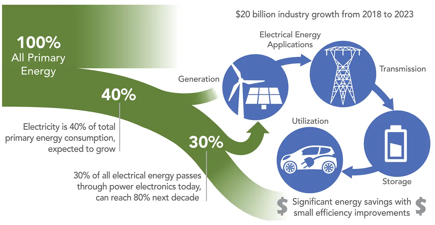
NLR's materials discovery and design work on ultra-wide bandgap (UWBG, E.g. > 3.4 eV) semiconductor focuses on epitaxial growth, high-performance device fabrication, and modeling from the materials to the package level.
Our research covers group III nitrides (GaN, AlGaN, AlN), gallium oxide (Ga2O3 and alloys) and related oxide and nitride compounds (such as ZnGeN2, InBO3, In2Ge2O7), and next-generation materials and includes wide bandgap (WBG, Eg > 2.7) semiconductors.
UWBG materials discovery and design research at NLR aims to develop materials and devices that can handle large power loads with low loss, often in extreme environments such as high temperatures, chemically aggressive atmospheres, and under significant radiation. These devices include power devices such as transistors, diodes, and next-generation extreme environment sensors.
Epitaxial Growth
We perform thin-film growth and characterization of homoepitaxial and heteroepitaxial layers of WBG and UWBG semiconductors for applications in electronic devices that can operate at extreme conditions. Growth methods include molecular beam epitaxy (MBE) and pulsed laser deposition. We have three MBE tools dedicated to nitride discovery, group III-N growth, and UWBG oxides (including Ga2O3, NiO, and others). These growth techniques enable high-quality materials and interfaces between functional semiconductor/insulator/metal layers, which are critical for reliable material and device performance.
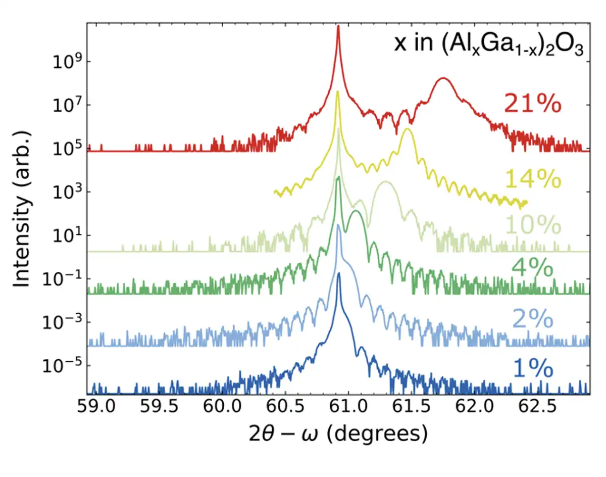
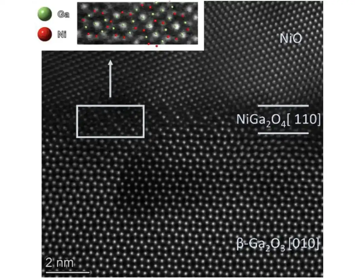
An example is given below, where MBE was used to grow a series of Al-substituted Ga2O3 thin films up to 21% Al. Substituting Al into Ga2O3 is used to increase the bandgap, decrease leakage current, and create modulation-doped field effect transistors. Another focus area is heteroepitaxial growth of p-type oxide semiconductors used in conjunction with n-type Ga2O3, which is not able to be p-type doped. Examples of these compounds include NiO and Mg:Cr2O3, among others.
For more information, see:
Epitaxial (AlxGa1−x−yIny)2O3 Alloys Lattice Matched to Monoclinic Ga2O3 Substrates, Applied Physics Letters (2024)
Rapid Screening of Molecular Beam Epitaxy Conditions for Monoclinic (InxGa1−x)2O3 Alloys, Journal of Materials Chemistry A (2024)
Structure, Defects, and Optical Properties of Commensurate GaN/ZnGeN2/GaN Double Heterojunctions, Journal of Materials Chemistry C (2023)
Growth and Characterization of Homoepitaxial β-Ga2O3 Layers, Journal of Physics D: Applied Physics (2020).
Device Fabrication
NLR's research in this area includes fabrication and characterization of first-of-a-kind device prototypes based on new ultra-wide bandgap semiconductor materials. Our extensive clean room fabrication capabilities include photolithography mask aligners, wet and dry etching stations, metallization, and dielectric deposition capabilities.
Device characterization efforts feature conventional probe stations with suitable electronics as well as low-temperature and high-temperature measurement capabilities.
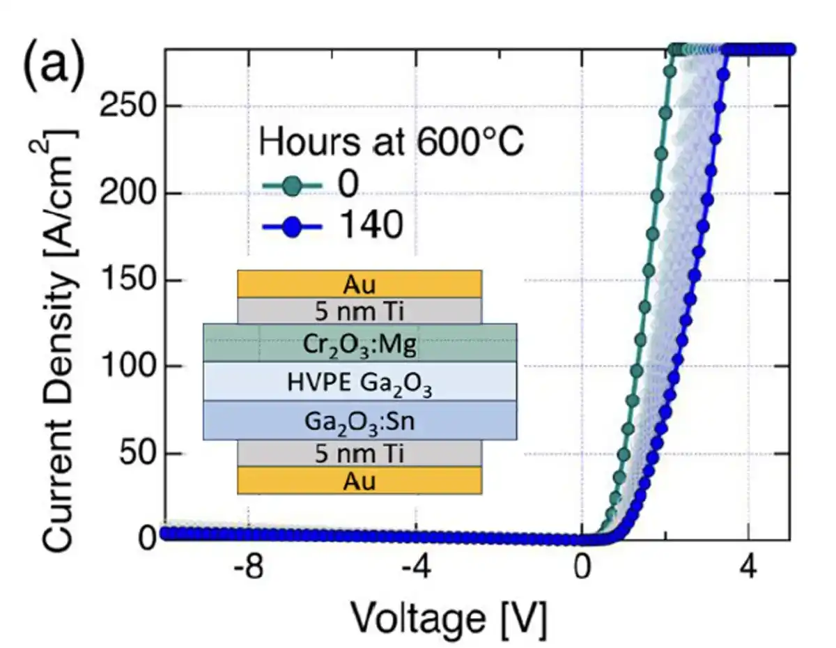
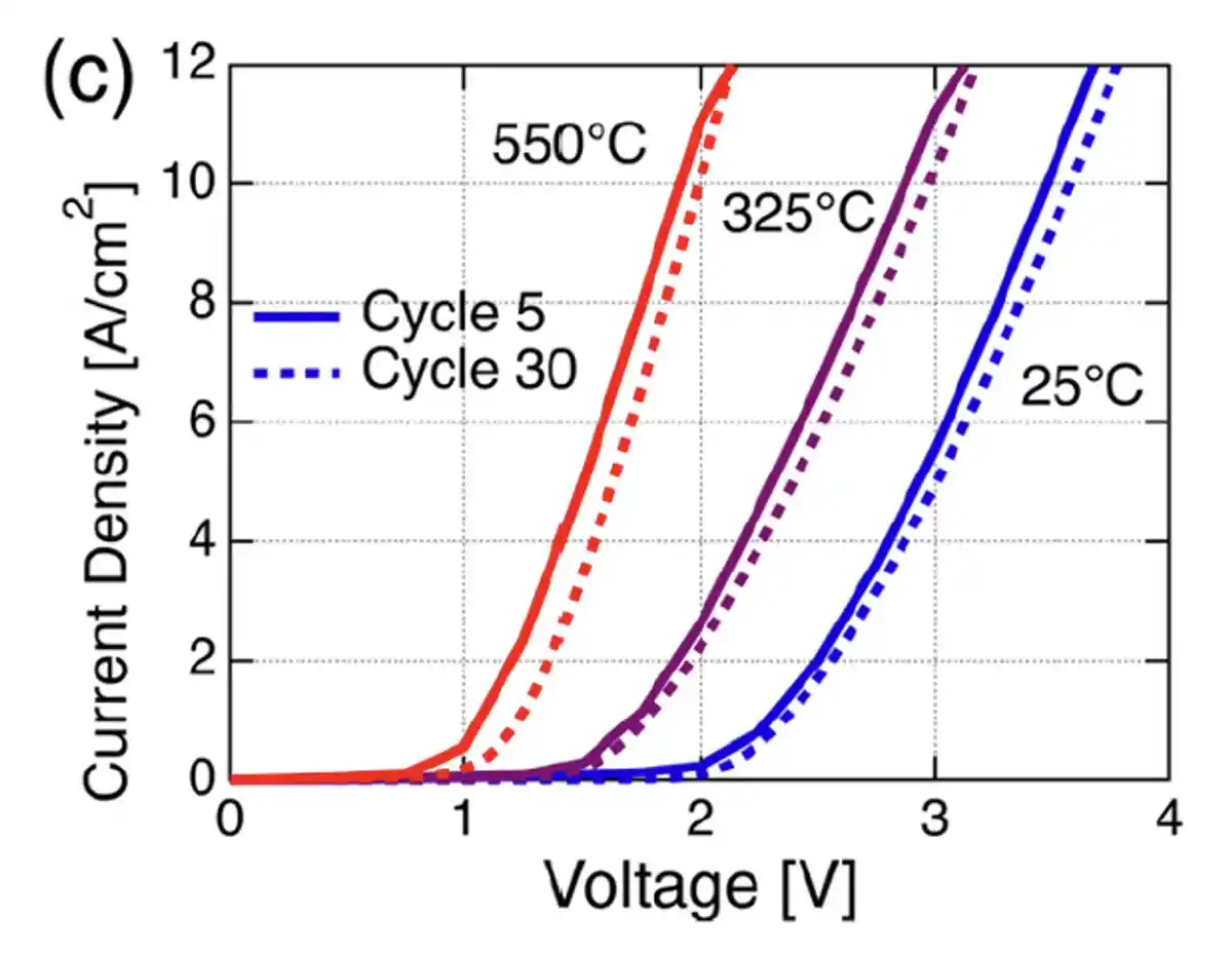
Using this device expertise, we are exploring a variety of applications, including long-term characterization of an oxide p-n heterojunction consisting of Mg:Cr2O3 on Ga2O3 that operated in a stable manner after exposure to 500°C for hundreds of hours and tens of cycles.
For more information, see:
NiGa2O4 Interfacial Layers in NiO/Ga2O3 Heterojunction Diodes at High Temperature, Applied Physics Letters (2024)
Ultrathin Stable Ohmic Contacts for High-Temperature Operation of β-Ga2O3 Devices, Journal of Vacuum Science & Technology A (2023)
Gallium Oxide Heterojunction Diodes for 400 °C High-Temperature Applications, Physica Status Solidi (a) (2023)
Novel Substrates
A key limitation in the establishment of any UWBG system is the availability of lattice-matched substrates or templates for epitaxial layer growth. Some promising material systems, such as high-aluminum content AlGaN alloys, have yet to realize their full potential due to a lack of lattice matched substrates.
NLR materials discovery and design researchers are solving this issue through novel carbide, nitride, and boride substrates and buffer layers which are lattice-matched to a wide range of III-N materials. These materials can eliminate the need for costly and thick metamorphic buffer layers, which result in poor device quality and cracks due to thermal mismatch.
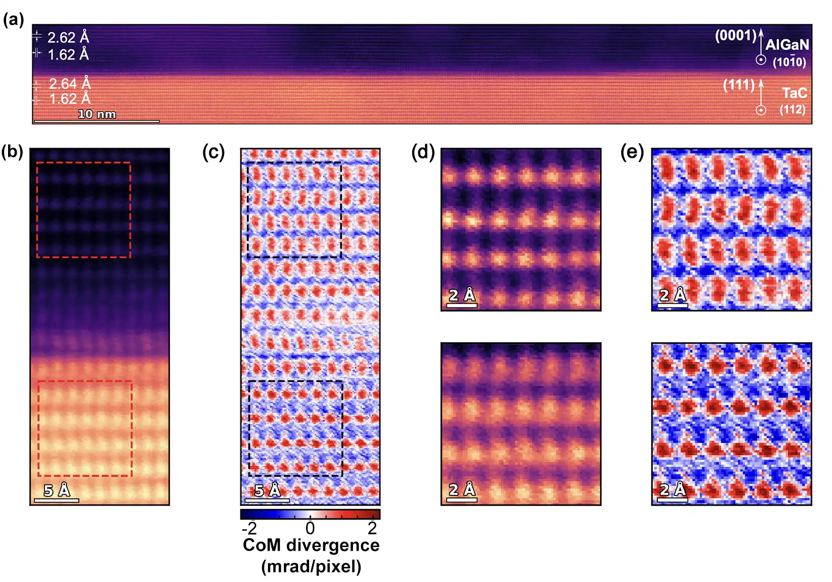
For more information, see Designing TaC Virtual Substrates for Vertical AlGaN Power Electronics Devices, PRX Energy (2024).
Computational Predictions and Experimental Validation of New Ultra-Wide Bandgap Materials
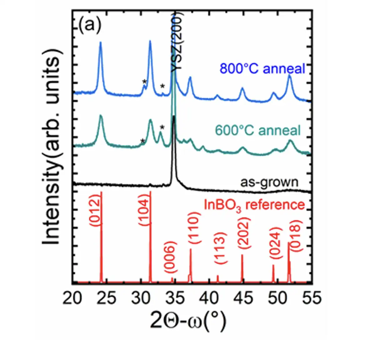
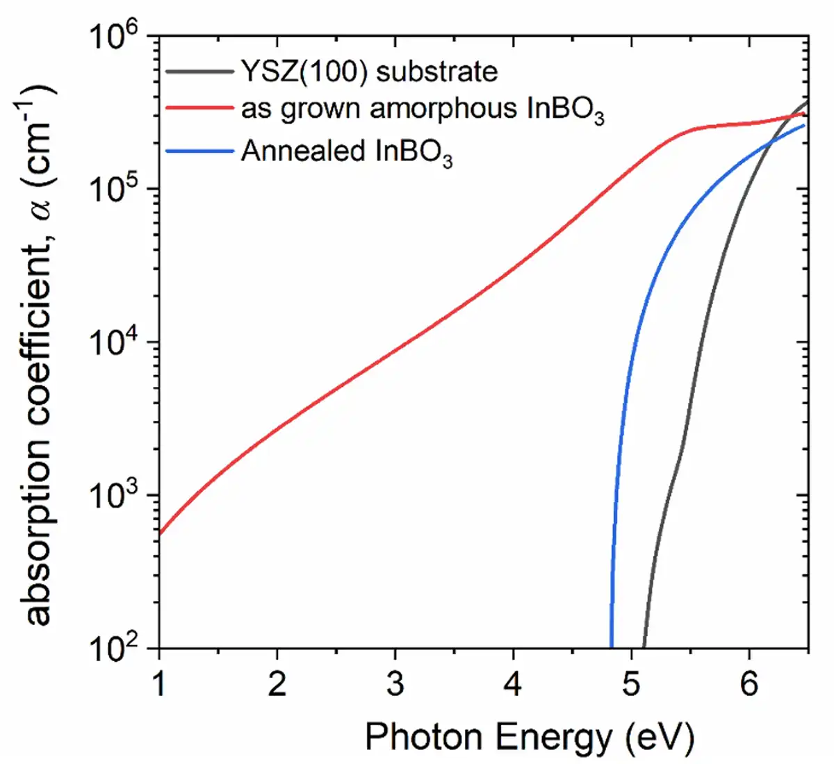
In collaboration with the Colorado School of Mines, we are predicting new UWBG semiconductors and experimentally validating their structure and properties. Recent examples include InBO3, In2Ge2O7, and related materials.
For more information, see:
Computational Identification of Ternary Wide-Band-Gap Oxides for High-Power Electronics, PRX Energy (2022)
Defect Chemistry and Doping of Ultrawide Band Gap (III)BO3 Compounds, Chemistry of Materials (2023)
A Computational Survey of Semiconductors for Power Electronics, Energy & Environmental Science (2020)
Electrothermal Modeling and Technoeconomic Analysis
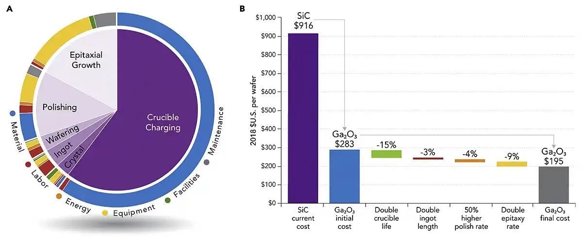
We are collaborating with other directorates at NLR in simulating the expected power electronic device performance, designing device packaging for its reliability, modeling thermal performance of the packages, and evaluating future cost reduction potential of UWBG materials.
For more information, see:
How Much Will Gallium Oxide Power Electronics Cost?, Joule (2019)
Projected Cost of Gallium Oxide Wafers from Edge-Defined Film-Fed Crystal Growth, Crystal Growth & Design (2022)
Computational Insights into Phase Equilibria between Wide-Gap Semiconductors and Contact Materials, ACS Applied Electronic Materials (2024)
Modeling and Analysis of Gallium Oxide Vertical Transistors, ECS Journal of Solid (2019).
Projects
Ultra-wide bandgap material and device research at NLR has been funded by the U.S. Department of Energy (DOE) and NLR's Laboratory Directed Research and Development (LDRD) Program.
This program was funded by DOE SC to advance transformational manufacturing techniques surrounding critical interfaces in next-generation power electronics materials and devices.
This program was funded by NLR's LDRD program to explore synthesis, dopability, and devices using InBO3.
This program was funded by DOE to create extreme environment hydrogen sensors using Ga2O3 and to develop methods for AI- and ML-guided advanced qualification of these sensors.
This program was funded by NLR’s LDRD program to develop growth methods for (Al,In,Ga)2O3 alloys.
This transformational LDRD program was aimed at developing NLR capabilities to integrate power device prototypes into functioning power modules.
This project was funded by DOE to demonstrate Ga2O3 materials and devices suitable for operation at high temperature (600⁰C) in extreme environments (corrosive atmosphere, mechanical stress).
This program was funded by NLR's LDRD program to demonstrate oxidation-resistant wide-bandgap semiconductor materials for electronic devices that can operate at high temperature. The specific goals were to fabricate and characterize Ga2O3 diodes during operation at 500°C in ambient atmosphere and to demonstrate proof-of-concept transistors based on new oxide semiconductors.
Research Collaborators
Nancy Haegel – Director of A Center for Power Electronics Materials and Manufacturing
Stephan Lany – Theoretical/computational
Vladan Stevanovic - Theoretical/computational (Mines)
Drew Haven – Single crystal growth (Luxium Technologies)
Michael Spencer – APEX deputy director (Morgan State University)
Tyrel McQueen – Single crystal substrate growth (Johns Hopkins/Paradim)
Heather Splawn – Hydride vapor phase epitaxy (Kyma Inc.)
Patrick Hopkins – Thermal transport (University of Virginia)
Contacts
Share
Last Updated Dec. 10, 2025
