Scanning Electron Microscopy
NLR's scanning electron microscopy (SEM) tools and techniques allow for routine and powerful analytical experiments to be conducted on a wide range of energy materials.
SEM scans a high-energy (0.1-30 keV) beam of electrons across a sample, which generates a variety of interactions and characteristic signals. Some of these signals include secondary electrons and backscattered electrons for different methods of imaging, and X-rays for energy-dispersive X-ray spectroscopy (EDS or EDX).
Additionally, an SEM can be utilized as a base for additional tools, such as pairing the electron column with an ion column to create a platform for focused ion beam-SEM (FIB-SEM) milling.
Techniques
A focused ion beam-scanning electron microscope (FIB-SEM) is a powerful tool that merges the functionalities of FIB milling with high-resolution SEM imaging, allowing you to not only image a material's surface but also prepare site-specific regions for cross-sectional imaging.
Common Uses
Cross-sectional analysis: FIB-SEM lets you mill into a sample, allowing imaging of internal and buried features of interest.
3D reconstruction: By capturing many cross-sections at different depths and stitching them together digitally, you can generate a 3D model of the material's internal structure.
High-resolution imaging: The SEM component provides exceptional magnification, allowing you to examine features as small as a few nanometers.
Chemical analysis: combining FIB-SEM with EDS and electron backscatter diffraction capabilities can identify the elemental composition and crystalline microstructure of specific regions within the sample.
Site-specific preparation: FIB-SEM allows for the precise removal of material to prepare electron-transparent specimens for scanning transmission electron microscopy analysis.
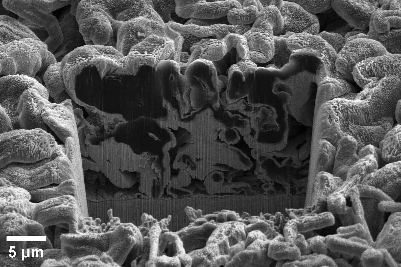
SEM image of electroplated Li metal after being cross-sectioned by a FIB
Energy-dispersive X-ray spectroscopy (EDS or EDX) is an analytical technique used for the elemental characterization of a sample. It works by detecting the characteristic X-rays emitted from a specimen when it is bombarded with high-energy electrons. Key principles include:
X-ray emission: When a high-energy electron beam interacts with the atoms in the sample, it can eject inner-shell electrons. The vacancies left by these ejected electrons are filled by electrons from higher energy levels, resulting in the emission of X-rays with characteristic energies specific to each element.
X-ray detection: These characteristic X-rays are detected by an EDS detector, which measures their energies and intensities to identify and quantify the elements present in the sample.
EDS is typically combined with either scanning electron microscopy (SEM) or scanning transmission electron microscopy imaging to perform elemental mapping from the microscale all the way down to atomic resolution.
Common Uses
Elemental mapping: By scanning the electron beam across the sample and detecting the emitted X-rays at each point, an elemental map can be created, showing the spatial distribution of elements within the sample.
Quantitative analysis: EDS can provide quantitative information about the elemental composition of a sample, including the relative concentrations of different elements.
Phase identification: EDS can be used to identify different phases or compounds within a sample by their unique elemental signatures.
 SEM-EDS mapping displaying the distribution of oxide species (cyan) within a silver
(purple) grid finger contact on top of a silicon (yellow) solar cell.
When an electron beam travels into a crystalline material at just the right angle (near a Bragg angle), the electrons penetrate deep into the crystal lattice through a mechanism called electron channeling. By purposely tilting the crystalline sample, specific channeling conditions can be satisfied such that any small deviation from the perfect crystalline lattice will locally increase the yield of backscattered electrons. Using a backscattered electron detector, typically positioned directly underneath the pole piece, images highlighting crystalline imperfections (e.g., dislocations, stacking faults) are produced.
Common Uses
Identifying crystalline defects: Defects such as dislocations, stacking faults, twin boundaries and grain boundaries can significantly impact material properties.
Quantitative defect analysis: Electron channeling contrast imaging (ECCI) allows for both qualitative and quantitative evaluation of crystalline defects, such as dislocation density.
Investigating interfaces: ECCI is useful for studying the defects that form at the interface between different materials, providing valuable insight into heteroepitaxial thin films.
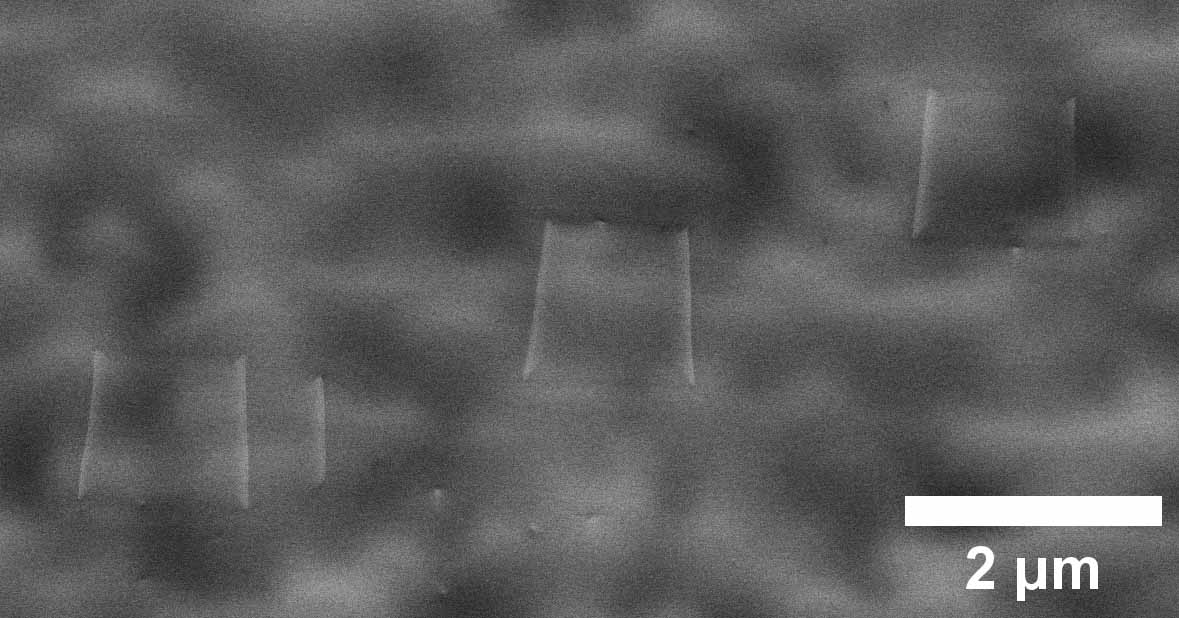 ECCI micrograph showing stacking faults (lines) and threading dislocations (dots) in a defective gallium arsenide thin film.
Electron backscatter diffraction (EBSD) is a powerful technique that utilizes a scanning electron microscope to spatially map out the crystalline microstructure of a sample surface. As the electron beam scans across the sample, each scanned point produces a diffraction pattern representative of the crystal structure at that precise location. Each of these diffraction patterns are indexed to a particular crystal structure and crystallographic orientation to build up an EBSD map rich in crystallographic information.
Common Uses
- Crystalline phase identification: Quickly identify the different crystallographic phases present in your sample, providing insights into its microstructure and properties.
- Grain structure analysis: Visualize and quantify the size, shape, and orientation of individual grains within the material.
- Boundary characterization: Study interface and boundary characteristics and distinguish between different types of grain boundaries (high-angle, low-angle, twins).
- Misorientation mapping: Measure the local variations in crystallographic misorientation across the sample, providing valuable information on deformation processes and crystalline defect density.
- Texture analysis: Determine the preferred crystallographic orientation of grains, influencing properties like strength and electrical conductivity.
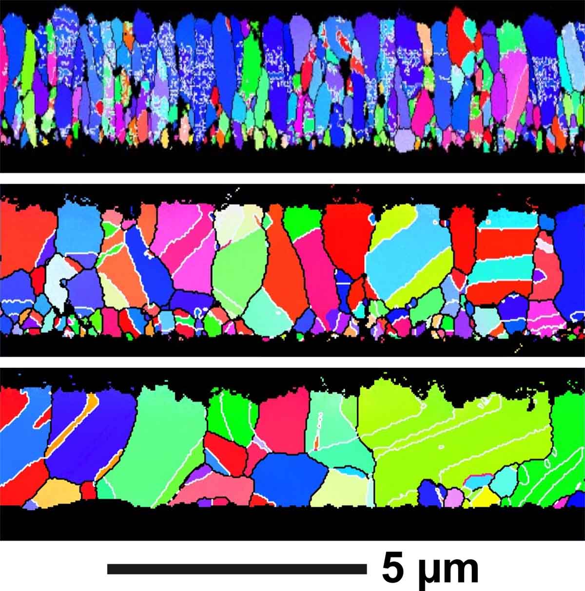
EBSD inverse pole figure maps showing the microstructure and crystalline texture of a series of cadmium telluride films processed under different conditions.
In presence of an electrostatic field (e.g., p-n junction, Schottky contact), electron-hole pairs excited by the electron beam can be collected and the resulting current measured with a current amplifier. Electron beam induced current (EBIC) provides information about the location of the junction, estimates of diffusion length, and surface recombination.
EBIC mapping reveals spatial variations in current collection due to defects such as grain boundaries, dislocations, and precipitates due to local changes in the band structure that define carrier recombination behavior. Dislocation density in semiconductors can be determined with very high precision in the 104–107 cm-2 range.
EBIC observations can also be conducted at temperatures between 15 K and 300 K, which alters the recombination behavior and can reveal information about defect energy level positions and density.
Common Uses
- Mapping the electrical properties of semiconductor materials
- Studying the effects of defects on the electrical properties of materials
- Characterizing the performance of solar cells and other optoelectronic devices
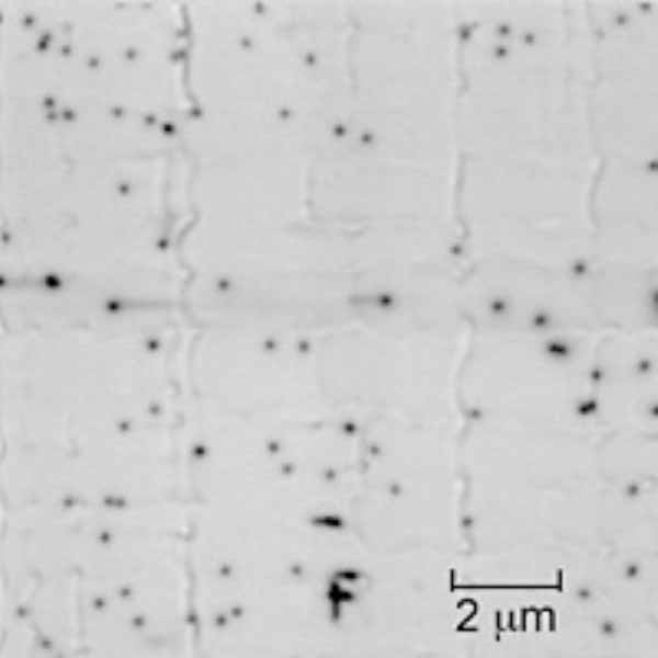
EBIC image of a gallium arsenide phosphide-on-silicon solar cell revealing threading dislocations (dark spots) crossing the p-n junction.
Recombination of excess carriers in electronic devices can occur non-radiatively through deep levels and generate heat in the semiconductor as well as radiatively through energy levels closer to the conduction or valence band edges. In the latter case photons are emitted and understanding the spatial distribution, relative intensity, and spectral character of these photons can provide valuable information about the quality of photovoltaic absorber materials and potential performance limitations.
When excited by an electron beam the resulting emission is called cathodoluminescence (CL). Synchronizing the scanning of the electron beam allows for mapping of this emission from sample. Directing the emission to a spectrometer enables spectrum-per-pixel acquisition. This provides information about the local bandgap, defect energy levels, and the spatial distribution of various radiative and non-radiative recombination centers.
CL spectrum imaging can be performed between 6K and room temperature with detection sensitivity in from 250 nm to 1600 nm. The spatial resolution can approach 10s of nm for some samples and the mapped area can range up to 50 x 50 μm2.
Common Uses
- Panchromatic imaging with germanium photodiode for emission intensity maps
- Spectrum-per-pixel mapping with a silicon charge-coupled device and indium gallium arsenide detectors (250 – 1600 nm)
- Mapping of the photon energy and full-width-half-maximum of selected radiative transitions
- Identification of energy levels and spatial distribution of extended defects and impurities
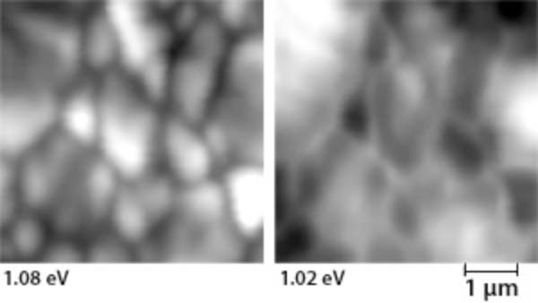 Photon intensity maps for different transitions identified on the emission spectrum of copper indium gallium diselenide thin films. Grain boundaries show a distinct electronic behavior.
Tools
Contact
Share
Last Updated Dec. 7, 2025
