Research
APEX hypothesizes that breakthroughs in power electronics functionality and reliability can be realized by understanding interface design principles and developing transformative manufacturing pathways that unlock broader materials choices for heterogenous integration.
We seek to enable these breakthroughs through foundational research to advance new materials and interfaces and understand and elucidate the chemical, physical, thermal, and electrical requirements at dissimilar interfaces.
Aim 1: Power Electronics Interface Co-Design for "A on B"
Accessing a broader range of "A on B" materials combinations will require new strategies for integration beyond epitaxial growth of layer A on lattice-matched substrate B. Interfaces are often integration-limited, where a mismatch between lattice constants and chemistries of A and B can produce undesired defects and accelerate performance degradation. At the same time, R&D is often limited to established combinations of materials under laboratory conditions, without considering long-term operation under harsh conditions, like in power electronics. Thus, the ability to tailor interface structure, chemistry, and properties is ever more important for realizing desired functionalities and performance under real-world operation conditions.
Knowledge of the interface structure on an atomistic level, as well as the interdiffusion or reaction products that may occur there, is critical for a mechanistic understanding of interface behavior. Developing new interface design strategies for combining dissimilar materials could expand material options for next-generation power electronics.
Aim 1 will build out the conceptual co-design groundwork needed to overcome limitations in the choice of the best materials combinations for aluminium gallium nitride (AlGaN), silicon carbide (SiC), and gallium oxide (Ga2O3) power electronics technologies, while taking into account nonidealities and real-world operation conditions.
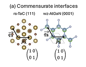
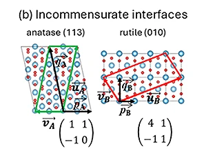
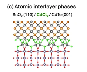
Interfaces can be designed via several approaches, based on the details of the structure and chemistry of the two initial layers being combined. Aim 1 conceptualizes heterogeneous interfaces in three categories with a hierarchy of increasing complexity (depicted below). These categories structure the formulation of science questions and associated hypotheses.
For more information about the research in Aim 1 or to discuss potential collaboration, please contact Stephan Lany at NLR.
Aim 2: Synthesis of "A on B"
The goal of Aim 2 is to synthesize "A on B" to enable transformative manufacturing that removes today’s "tyranny of the substrate," where achievable properties of both materials and devices are severely limited by the small subset of possible substrates. Rather than addressing just the epitaxial active layer properties, APEX will focus on substrate and template innovation. This research will be enabled by one of the few laser-heated bulk crystal growth tools in the world at John Hopkins University, APEX partner, to synthesize metal diborides and carbides with metallic conductivity that could enable vertical device architectures and reduce thermal losses. These materials are ideal partners for the already established AlGaN ultra-wide bandgap (UWBG) system and offer exceptional lattice and thermal expansion matching (see figure below).
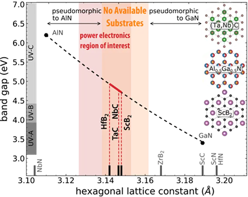
For more efficient, higher performance power electronics, excellent electro-thermal transport across interfaces and interface stability is needed, as well as a vertically conducting architecture to handle large currents. By expanding materials and interface design options for "A on B" integration, we can potentially meet both these needs and remove performance and manufacturing bottlenecks. The transformational manufacturing approaches in Aim 2 and Aim 3 will use AlGaN as a model system due to the significant impact that AlGaN could have on power electronics.
The primary loss mechanism in emerging high-current, vertically conducting power electronics is often resistive loss in the substrate itself. Aim 2 will investigate the materials and interface science to enable solutions that significantly decrease the thermal load while simultaneously improving performance. This will be accomplished by (a) targeting "B" layers that have metallic conductivity (>100x improvement over semiconducting silicon, SiC, or gallium nitride, GaN) and do not contribute significantly to I2R heating and (b) identifying effective methods to remove the active layer from the substrate, enabling a direct bond to the package heat sink.
Aim 2 is based on the related hypotheses that materials exist that can fill the "lattice-matched substrate gap." Challenging synthesis issues with these substrates can be overcome with recent advances in floating zone bulk crystal growth, and substrate removal and layer transfer could enable a significant new co-design space. Specific questions we will address include:
- Can crystal orientation, quality, defects, dislocations, and properties of bulk boride and carbide substrates reach metrics that enable low-defect-density, lattice-matched AlGaN growth?
- Can the chemically and structurally heterogeneous interface between a boride/carbide and AlGaN be controlled without generation of unwanted defects and deleterious phases?
- What is the impact of various III-N substrate removal and layer transfer techniques on interfaces and defect formation, and how do they impact real-world resilience?
For more information about the research in Aim 2 or to discuss potential collaboration, please contact MVS Chandrasheker at Morgan State University.
Aim 3: Transformative Manufacturing: "A on B" at Speed and Scale
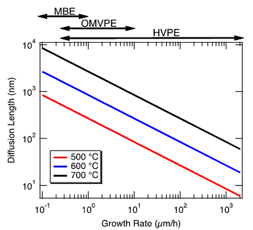
In Aim 3, APEX will perform foundational science to enable future scalable, cost-effective integration of the discoveries in Aims 1 and 2 into power electronics manufacturing using hydride vapor phase epitaxy (HVPE). Molecular-beam epitaxy and organometallic vapor phase epitaxy are used for materials synthesis in commercial microelectronics but are cost-prohibitive for the thick drift layers needed for high-power applications due to low growth rates and throughputs.
HVPE was developed in the 1960s and is commercially used to produce III-V phosphide LEDs, bulk GaN substrates, and thick templates of GaN and Ga2O3 for use in power electronics and LEDs. This makes HVPE a commercially proven epitaxial growth option with demonstrated high-throughput deposition of III-V nitride and Ga2O3, with the potential to deposit a wider range of materials in the future. HVPE's unmatched growth rates and high material quality make it the ideal growth technique to deposit thick, low-doped drift layers.
Despite HVPE's high-throughput capabilities, limitations with the formation of heterointerfaces have prevented it from being used in manufacturing to make most device layers. In traditional HVPE, switching between the growth of two different materials requires a "growth interrupt," during which impurities can accumulate on the surface, leading to defective interfaces. D-HVPE uses substrate motion at high temperature between different growth chambers to remove this limitation. This leads to the successful growth of abrupt and defect-free interfaces and could be applied for nitride materials. However, heterointerface initiation for III-N materials in HVPE is not well understood. Research on the growth fundamentals (kinetics, defect studies) is necessary to develop synthesis control and material quality of AlGaN to be used in next-generation power electronic devices.
Development of these diagnostic tools will support the synthesis and integration of the novel substrates and materials produced in Aim 2 and will provide fundamental insight into growth kinetics relevant to the interface simulation in Aim 1. We will use this information, along with data from growth studies, to build kinetic models of the various processes that control growth. This will allow us to manipulate the growth kinetics to overcome anticipated limitations of growing relevant materials on new templates—for example, developing pure phases of traditionally unstable III-N alloys, using HVPE's high growth rates (see figure below), and growing on less traditional substrates. Kyma’s demonstrated growth technique to reduce Si and other background impurities should result in UWBG semiconductor films with enhanced mobility and breakdown fields, building upon the advantage of the APEX-enabled lattice-matched substrate. This will result in material properties ideal for integration into future power electronic devices.
Aim 3 will address these science questions:
- What are the relevant species in the AlGaN HVPE growth environment, and how can their kinetics be manipulated to increase growth rate?
- How can we use growth rate to control and prevent phase separation in metastable alloys?
- Can nitride growth by HVPE on novel lattice-matched substrates lead to improved UWBG semiconductor electrical and thermal properties?
The APEX team has decades of experience in growth and materials characterization by HVPE. Kyma's HVPE process capabilities have been developed and advanced for more than 20 years, and its HVPE reactor technology is in its 16th generation of refinement. NLR work in advancing dynamic interface control in D-HVPE opens significant potential for transformative manufacturing. Team members also have experience in equipment design and modification, which will be critical to generating new analytical tools and integrating new materials into future manufacturing processes. The results from Aim 3 will ensure that the knowledge developed in APEX has a pathway via a proven and potentially transformative manufacturing environment for power electronics in the future.
For more information about the research in Aim 3 or to discuss potential collaboration, please contact John Simon at NLR.
Aim 4: Interface Characterization and Real-World Resilience of "A on B"
Power electronics are critical components in delivering a future grid design that can nimbly handle higher power loads from intermittent and distributed sources. But given increasingly demanding operating requirements, they may also be one of the potential weakest links. In an ideal world, these materials, devices, interfaces, and packages would be able to withstand high temperatures (~400°C), higher voltages (~ up to 50 kV), and higher power densities (~ up to 1000 W/cm2), well beyond what is achievable today. It is not sufficient to envision or even form ideal "A on B"; we must co-design for real-world resilience. At all parts of the stack in power electronic devices, it is the interface where most of the losses occur, resulting in thermal buildup, decreased performance, and a breakdown in resilience. Aim 4 will address life cycle and resilience challenges at the heterogeneous interfaces through state-of-the-art nanoscale correlated characterization of structural, electronic, and thermal properties.
Lattice defects and disorder can act as scattering centers for electrons and phonons, increasing thermal resistance, and, as discussed in Aim 1, new phases or interphases can also form at interfaces between layers with different structural, chemical, and electronic properties. One common approach is to minimize defects by using lattice-matched substrates; however, as discussed in Aim 2, this greatly limits the current set of available materials. APEX proposes to flip the paradigm by designing the interphases so that they can actually contribute through stability design and targeted functionality.
The focus of Aim 4 is to characterize interphases with high spatial, chemical, spectral, and temporal resolution, providing knowledge and feedback to guide predictive control over synthesis products and device performance (see figure below).
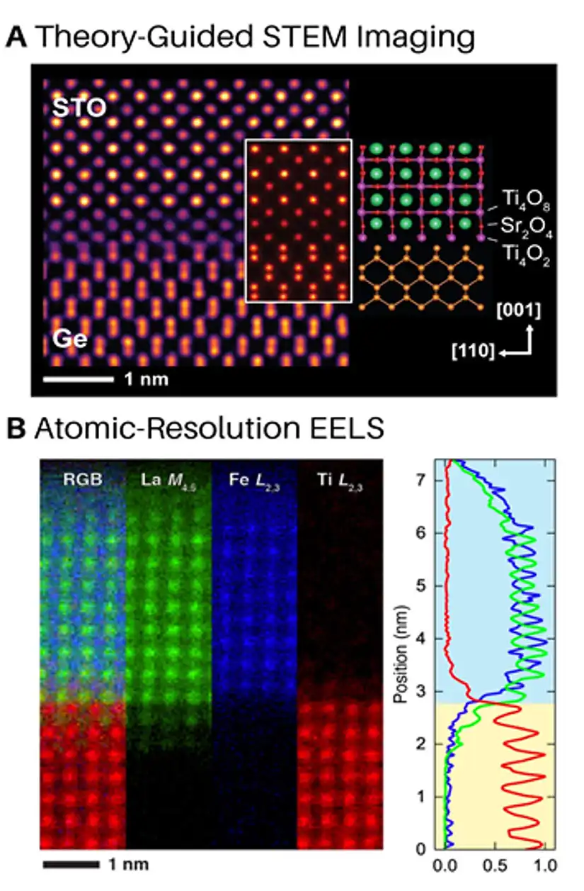
When two materials are brought into contact, the interface is rarely abrupt but instead occupies a finite spatial dimension up to several nanometers thick, depending on synthesis conditions. This region can be structurally, chemically, and electronically distinct and remarkably different depending on the stacking order. This is particularly true for the interface between dissimilar materials. Therefore, it is vital to identify and study the interphases that actually form and observe how they evolve. This will provide a framework to understand and control synthesis, mitigate degradation, and increase the life cycle of resulting devices.
Our overarching scientific questions are:
- What are the interphases that form between dissimilar materials for a given set of synthesis conditions?
- How do we tailor the electrical and thermal properties at the interphase (based on the defects and electronic and phononic interface properties) for superior performance?
- What is the subsequent environmental evolution of the interphase?
For more information about the research in Aim 4 or to discuss potential collaboration, please contact Jessica McChesney at Argonne National Laboratory.
Share
Last Updated Jan. 26, 2026
