Low-Cost III-V Solar Cells
NLR develops technologies to drastically lower the cost of III-V solar cells while maintaining their conversion efficiency, thus enabling their use in conventional flat-plate and low-concentration applications.
At present, the cost of these devices is very high, which limits their use to high-concentration and space applications. We address the two major costs in the production of high-efficiency III-V devices: the epitaxy and the single-crystal substrates used for growth.
Our Expertise
We have expertise in:
- Growth of III-V device structures using advanced hydride vapor-phase epitaxy (HVPE)
- Computational fluid dynamics and thermodynamic/kinetic reaction modeling
- Advanced semiconductor growth reactor design
- Processing, characterizing, and analyzing III-V materials and devices.

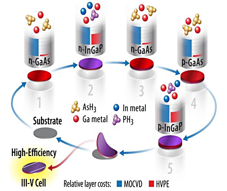
Schematic of an in-line HVPE reactor with continual substrate reuse that eliminates metal-organic sources and uses cheap elemental metals. The bar charts show the relative materials costs for each layer.
Research Areas
It is critical to lower the deposition costs of III-V photovoltaics, which are the most efficient solar cells available. This cost decrease will enable these thin, light, flexible, and stable devices to enter new markets and have a major impact on the production of electricity in applications where it is not currently feasible.
The first major cost in III-V devices is epitaxy, driven by the costs of the source materials and the relatively low throughput of current reactors. HVPE growth uses low-cost elemental source materials and has demonstrated high-quality III-V growth at rates that lead to the possibility of producing high-efficiency solar cells in less than a minute—compared to the hours it takes today.
The other major cost in the production of III-V devices is the substrate on which they’re grown. Typically, this is a perfect single crystal of GaAs or Ge, but both substrates are too expensive to enable widespread terrestrial use of III-V solar cells. Techno-economic analysis indicates that combining high-throughput, low-cost HVPE with low-cost substrates—while maintaining high efficiency—can lower III-V energy costs to levels suitable for one-sun and low-concentration markets.
In pursuit of this goal, our work addresses the costs of both the epitaxial growth of the III-V device layers and the substrates on which these layers are grown to lay the foundation for a competitive, impactful, U.S.-led III-V PV industry.
D-HVPE Growth of III-V Solar Cells
We are developing low-cost III-V PV using our innovative dual-chamber D-HVPE growth reactor that mimics an in-line production tool. We are able to create very abrupt doping and composition interfaces in our system, a capability that was previously quite difficult using HVPE growth. Using this system, we have demonstrated single-junction GaAs solar cells with >25% conversion efficiency grown and growth rates exceeding 5 micron per minute. We are developing monolithic two-junction devices with target efficiencies >30%, with three-junction devices being planned for the future. In addition, we are pursuing high-quality top cells for integration with high-efficiency crystalline Si solar cells with an expected tandem cell efficiency >30%.
Research involves understanding, improving, and extending capabilities of the D-HVPE growth process toward multi-layer structures using robust experimental methods and computation fluid dynamics models coupled to kinetic descriptions of the growth reactions. We also study the effect of particular device structures on overall performance using the quality of the HVPE-grown materials as inputs.
Decreasing Substrate Costs
We are also developing technologies that reduce the cost of the substrates used for III-V device growth, including controlled spalling of brittle materials, reformation of growth surfaces over porous materials, and growth on two-dimensional (2D) materials that enable low-cost substrate re-use and high-quality epitaxy. We work extensively with industry and academia to validate new substrate ideas and are continuously seeking new partners.
Tools and Capabilities
We use the following as we develop low-cost III-V device technology:
- Custom, dual chamber D-HVPE system capable of high spatial uniformity, sharp interfaces, very high growth rates, and high material utilization
- Cleanroom in which epitaxial wafers can be processed into full devices
- Suite of cell testing techniques, including current-voltage and quantum efficiency testing of full multijunction cells
- Computational fluid dynamics modeling software for understanding and improving growth systems, as well as developing next-generation growth reactors.
Contact
Share
Last Updated Dec. 6, 2025
