Capacitance Techniques
Capacitance techniques monitor the movement of electronic charge within a semiconductor device and provide a measure of free-carrier and electrically active defect-state properties.
Capacitance is the charge storage capacity and is measured across a rectifying junction.
Applications
Capacitance-Voltage Measurements

DLTS characterizes defect levels to assist in identification of impurities and potential recombination centers.
Determines the concentration of majority carriers in the bulk of the device, energy levels of interface states (or both) that often exist between the surfaces of dissimilar materials.
Deep-Level Transient Spectroscopy
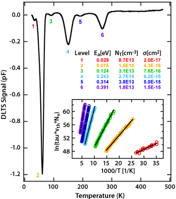
Examines the time-dependent flow of charge into and out of localized energy states associated with defects in the semiconductor. DLTS can detect trap concentrations as low as 1012 cm-3 and as high as the doping level (constant-capacitance DLTS). It also distinguishes between minority- and majority-traps; determines activation energy and captures cross-section. Our capabilities allow the use of electrical or optical pulses to fill traps and a sample temperature range of ~20 to 475 K. DLTS is a nondestructive complement to secondary-ion mass spectrometry and Auger electron spectroscopy.
Admittance Spectroscopy
Characterizes defect levels by measuring capacitance with varying frequency and temperature.
Share
Last Updated April 3, 2025
