
Researchers Determine Simplified Way To Make Perovskite Solar Cells by Coating Multiple Layers at Once
A concept developed at the National Renewable Energy Laboratory (NREL) simplifies the process to manufacture perovskite solar cells, which could accelerate the path toward commercialization of the technology.
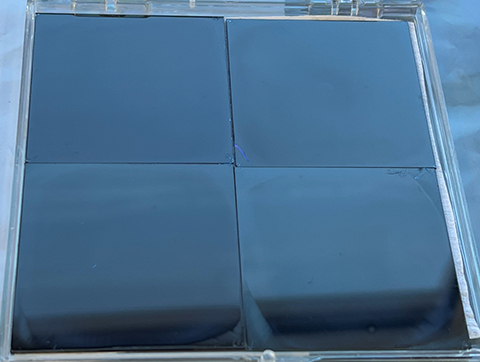
Perovskite solar cells are made by sequentially depositing various layers onto a conductive glass substrate, requiring multiple coatings to create the necessary full device structure. The new technique eliminates or combines some of those steps, thereby simplifying the manufacturing process, which could lead to yet lower manufacturing costs.
NREL researchers were able to make these high-efficiency perovskite solar cells without
certain steps.
Perovskite solar cells are composed of a perovskite light-absorbing layer and adjacent layers that extract positive and negative charges on opposite sides of the perovskite when light is absorbed. One of these layers, called the hole-transport layer (HTL), is used to extract positive charges. Perovskites can be made without an HTL, but such devices’ efficiency lags that of the full perovskite solar cell device structures.
The team produced a high-efficiency solar cell that retained more than 90% of the initial efficiency after 1,200 hours of continuous operation.
Xiaopeng Zheng, a postdoctoral researcher in the Chemistry and Nanoscience Center at NREL, reports in Nature Energy how a one-step solution-coating procedure allowed two separate layers, namely the HTL and perovskite absorber, of a solar cell to spontaneously form with only one coating step, eliminating the separate hole-transport layer fabrication. Instead, as the paper points out, the chemical solutions form “a robust self-assembled monolayer simultaneously as an excellent hole-selective contact while the perovskite crystallizes.”
Zheng said the new, simplified process to make the HTL and perovskite simultaneously reduces the number of coating and heating steps and removes the need for expensive HTL materials.
“It is challenging to uniformly manufacture a thin HTL layer using the scalable solution method, and this may be also a barrier to commercialization,” Zheng said. “Our approach could also avoid this problem.”
He estimated that removing the steps previously needed to create the HTL and then having to heat it up could cut the solution-processing time by a third.
“Even if we didn’t save a lot of time here, it brings about the notion that the manufacturing process could be reevaluated with this new concept in mind,” said Joseph Luther, a corresponding author of the paper and senior research fellow within the Materials, Chemical, and Computational Science directorate at NREL. “Multiple processing steps could be combined; layers could spontaneously form. I’m not yet sure how one could coat all the layers at once, but this highlights that perhaps it could be done.”
In addition to Zheng and Luther, the paper, “Co-deposition of Hole Selective Contact and Absorber for Improving the Processability of Perovskite Solar Cells,” was co-authored by NREL colleagues Min Chen, Chuanxiao Xiao, Jay Patel, Darius Kuciauskas, Rebecca Scheidt, Steven Harvey, Brian Wieliczka, Ahmad Kirmani, and Michael McGehee.
Other researchers are from Hong Kong, Switzerland, and Lithuania, as well as from the University of Kentucky, the University of Toledo, and Brown University.
“While the initial discovery of the procedure was made at NREL, the co-authors from various other institutions find the same effects and strengthened the findings,” Zheng said. “We discovered and proved the concept at NREL, and quite a few other groups expanded this finding to be more universal with different perovskite compositions, HTLs, different solvents and various other coating styles. Such coordinated efforts are welcomed in the perovskite field. We believe this will allow this work to gain greater adoption.”
Understanding how the different layers crystallize was supported by the Center for Hybrid Organic-Inorganic Semiconductors for Energy (CHOISE), an Energy Frontier Research Center funded by the U.S. Department of Energy’s Office of Basic Energy Sciences, and the manufacturability and scaling work was supported by the department’s Solar Energy Technologies Office.
Last Updated Jan. 22, 2026