
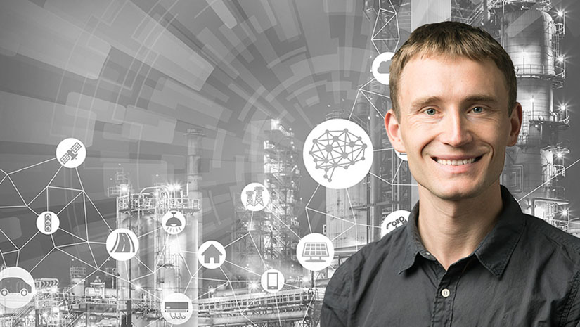
Q&A With Andriy Zakutayev: Materials Architect Builds New Energy-Efficient Devices One Atom at a Time
Manufacturing Masterminds Series
When you look at a computer, what do you see? Maybe you see a tool. Or just the physical parts, like a keyboard or a screen. But Andriy Zakutayev sees something nearly invisible: electrons, flowing behind all those physical components, reacting to each command with almost magical precision.
Andriy grew up in Ukraine. As a young tween, when his parents bought the family’s first computer, Andriy remembers looking at the boxy electronic, thinking, “How do you make electrons go where they’re supposed to go?”
The answer? Become a materials architect.
As a materials scientist at the National Renewable Energy Laboratory (NREL), Andriy manufactures materials—atom by atom—to find new ways to control these minute carriers of precious electricity. Right now, for example, he is researching new semiconducting materials, the foundation for the microchips that run most modern electronics, including computers, smartphones, battery controls, solar panels, lasers, lightbulbs, and much, much more.
Semiconducting materials, like glass or copper, either block or conduct electricity. But one superior kind of semiconductor—called ultrawide-bandgap semiconductors—could block huge amounts of voltage or conduct enormous currents without breaking. With such materials, we could build smaller, faster, more reliable, and more efficient electronics. And if scientists like Andriy can build semiconductors to survive superhigh electrical currents, corrosive environments, and extreme temperatures, these electron highways could save American businesses and consumers billions of dollars in energy costs.
“I am optimistic,” Andriy said, referring to the widespread use of ultrawide-bandgap semiconductors. “It will take a lot of diligent research, development, engineering, deployment, and reliability studies for that to happen. But I think the future is bright.”
In the latest Manufacturing Masterminds Q&A, Andriy explains how the ongoing war in Ukraine impacts his professional life, what it is like to spray-paint with atoms, and how materials can have memories. This interview has been edited for clarity and length.
What was it like growing up in Ukraine?
Growing up and studying in Ukraine taught me how to be resourceful—to get things done with the minimal resources that were available in the country at that time and to be grateful for what I have. I like to think that being resourceful in a more prosperous country, like the United States, translates into work efficiency, being productive, and not wasting the amazing resources we have available here.
How has the ongoing war in Ukraine affected you?
The war gets in the way of my professional efficiency and work-life balance. Every day, I feel torn between doing science to solve very important, long-term, worldwide energy and climate problems and then, in the evening, triaging urgent medical and protective gear requests from people defending the country where my family and friends live, as a part of the Sunflower Seeds Ukraine nonprofit.
Take us back a bit. How did you end up at NREL?
I always saw the United States and its semiconductor industry as the place where an electrical engineer can make the most impact in the world. Then, when I came here for my doctorate, I was attracted to NREL for two reasons: the lab’s mission to advance energy efficiency, sustainable transportation, and renewable power technologies, as well as its historical, core strength in the design and discovery of new semiconductor materials for photovoltaic solar cells and other applications.
Now, you lead NREL’s materials discovery and design team. What are you and your team trying to accomplish and why?
Our overarching goal is to design and discover new kinds of materials to design more versatile and energy-efficient electronic technologies. We try to answer the question: How do we design materials to perform a specific function for a solar cell, power conversion transistor, circuit, fuel cell, or battery?
What kind of functions or properties are you trying to achieve?
That depends on the application. For one project, funded by the U.S. Department of Energy’s Advanced Materials and Manufacturing Technologies Office, we’re looking for semiconductors that can survive extreme operating environments and don’t catch fire, burn, decompose, or break.
But whether they can do that or not boils down to their material properties. For example, there is a semiconductor property called the bandgap, which defines what electrical power or temperature the semiconductor can operate at without breaking. If we want a high-power, high-voltage semiconductor, we search for materials with wide bandgaps (and a few other semiconductor properties). For materials that can operate in ambient air or corrosive conditions, we would look for rock-like materials made of oxygen and other very common elements in the Earth’s crust that have survived on this planet without decomposing for millennia.
Are you optimistic that wide-bandgap semiconductors could be widely used someday soon?
Yes, I am optimistic. You can now buy energy-efficient LED bulbs off the shelf. Those are made of specialty wide-bandgap semiconductors. And many new electric vehicle models use wide-bandgap semiconductors to convert DC into AC voltage. And I think we are on the right trajectory that, some 10 or 20 years from now, you’ll see advanced ultrawide-bandgap semiconductors in very large-scale applications, like the electrical grid.
In your NREL profile, you describe your research as “materials discovery and design.” What do you mean by that?
This is an oversimplification, but since the Stone Age and until a few years ago, people collected and poked rocks to see which ones do what. Materials design is the other way around. It puts material functionality and property first and then finds the right material that has that functionality.
To construct a building, architects don’t just throw together bricks and rocks and steel they find lying around. They have an idea of what they want to build and the blueprints for how to build it. That architectural design logic translates to materials design. We have a material or a device in mind that we want for an energy application. Then we pick and assemble the elements to achieve the desired properties instead of just throwing a bunch of elements together and seeing what happens.
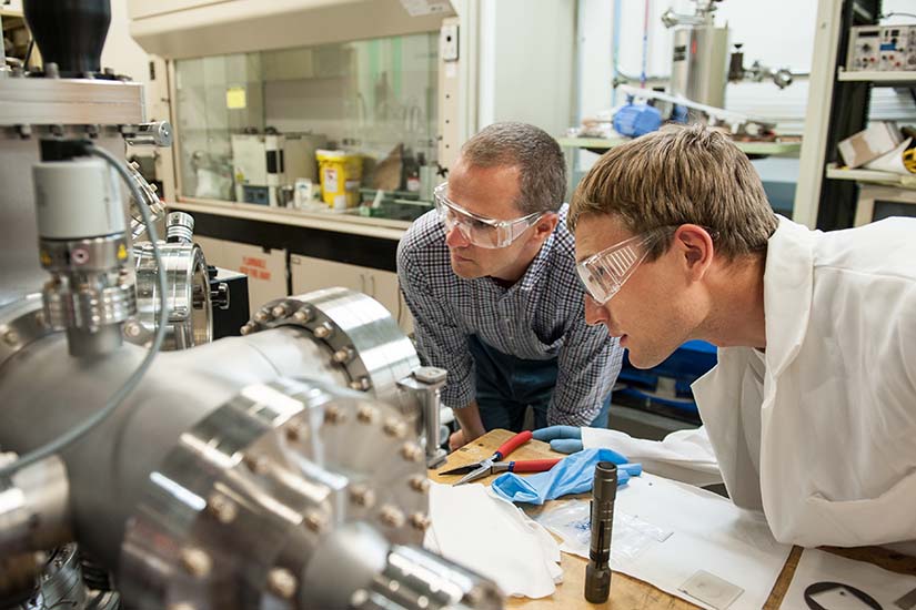
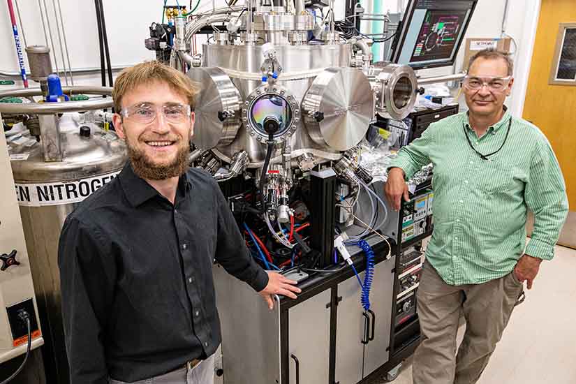
OK, but how do you do that—assemble atoms, one by one, into a material?
We often use what we refer to as atomic spray-painting. You can have two “cans” of material A and material B, and then you spray them together—not on the sheet of paper or a wall but, in our case, on a piece of silicon or glass. We even have special research samples. On one piece of glass, for example, you could have material A (like the color red) on one side and material B (like the color blue) on the other, and all possible A–B combinations, like a rainbow, in between. That lets us accelerate research, investigate more materials, and understand how their properties change.
Have you discovered any surprising properties through these experiments?
Materials science surprises us every day. Right now, one of the semiconductors I’m studying is gallium oxide. Some 10 or 20 years ago, people discovered you could modify this glass-like material and make it electrically conducting. That’s what we call an ultrawide-bandgap semiconductor. If you can control whether you have or don’t have electrons in that material, you could use it in power electronics or high temperature electronics. It’s like discovering a rock that does something the rock shouldn’t do—like a soft, squishy rock or a nugget of gold.
You mentioned that materials can have memories—can you explain that?
People figured out how to make efficient filters for 4G and 5G telecommunications out of a material called aluminum scandium nitride, a wide-bandgap semiconductor. And then boom, maybe 3 years ago, people discovered that this material can remember its electrical state. Like the digital memory bits in computers, you can electrically control these electrons.
That means you don’t have to keep supplying current or voltage for the material to remember—and maintain—its electrical state. And that’s very important. We could use this to design materials that use 10 times less electricity. That means a computer or smartphone battery would last for days instead of hours. But a lot more research must be done for that to happen.

In an ideal world, what would you hope to accomplish?
One very cool thing would be to have all electrical energy and all fuels come from renewable and sustainable sources, such as sunlight. That would require us to collect electrical energy through photovoltaic solar cells. But we would also need efficient ways to convert that electrical energy from AC to DC without losing much of it (like with ultrawide-bandgap semiconductors) and efficient ways to use it (like having semiconductor memories that don’t consume much energy).
That’s obviously a very grand vision, and it’ll take many years and decades to get to that. But I think we’re ready for the challenge and are on our way there.
What advice would you give to a young scientist who’s following in your footsteps?
Many people would answer, “Follow your dream,” in response to this question. I would add that it’s equally important to have a plan on how to achieve that goal in a way that makes the most impact, even if that requires you to adjust your original goal.
Interested in building a clean energy future? Read other Q&As from NREL researchers in advanced manufacturing, and browse open positions to see what it is like to work at NREL.
Last Updated May 28, 2025