
In Ultrathin Layers, NREL Researchers Find a Path to Better Materials
Unexpected Crystalline Structure Explains Mechanism of Long-Used Solar Cell Treatment and Hints That Further Materials Discoveries Await

For more than three decades, photovoltaic researchers have known that the addition of a single chemical—cadmium chloride—creates better-performing cadmium telluride (CdTe) solar cells. But they have not understood exactly why—until now. The answer has implications for materials science that stretch well beyond solar cells.
The light-absorbing layers in CdTe solar cells are composed of a thin film of material, about 10–100 times thinner than a human hair. Lots of modern devices, from solar cells to catalytic materials to organic light-emitting diode TVs, rely on thin-film materials. The surfaces at which these thin layers meet, or interfaces, are even thinner—100,000 times thinner than a human hair—and play a crucial role in the devices' functions. A better understanding of thin-film interfaces could improve how we fabricate many different materials, but the precise structure of interfaces at the atomic scale is often difficult to study.
A Proven, But Unexplained, Boost for Solar Cells
In CdTe solar cells, the electrical charges created by an absorbed photon can be trapped and lost at the interfaces between the light-absorbing layer and the layers that carry those charges away into electrical circuits. As early as the 1980s, CdTe researchers realized that treating the interfaces in the solar cell with a small amount of cadmium chloride (CdCl2) could reduce the loss of charges at the interfaces and improve the solar cell's power conversion efficiency.
Clearly, the addition of CdCl2 changed the interface in a crucial way. But further experiments could not resolve the interface's structure down to the atomic level to explain why the CdCl2 treatment was so effective. This challenge is not unique to CdTe solar cells. Interfaces are notoriously difficult to study and understand at the atomic level, especially in cases of nonideal interfaces between materials that have different crystal structures.
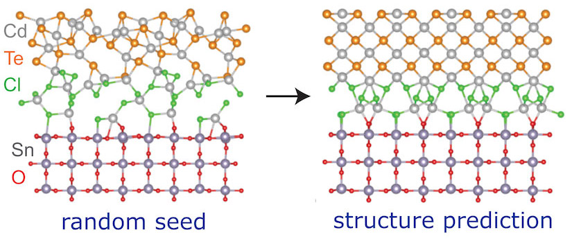
Modeling Offers New Insights Into Interfaces
A new approach from a team of National Renewable Energy Laboratory (NREL) researchers and colleagues at Khalifa University, Bowling Green State University, and First Solar—an American CdTe solar manufacturer—has unmasked the details of the CdCl2 interface treatment. By modeling the behavior of individual atoms and electrons, the team simulated possible arrangements for CdCl2-treated interfaces.
To calculate the electronic structure of a CdTe solar cell—and thereby determine its charge collection—the researchers first needed to determine the atomic arrangement CdCl2 interface, which had never before been done for CdTe solar cells. To achieve this, the team implemented a structure prediction algorithm for interfaces. The algorithm began with a random arrangement of atoms and then allowed them to settle, using a method called density functional theory to calculate the atomic forces. The algorithm repeatedly made small but realistic changes to the positions of the atoms at the interface, which allowed the team to identify the lowest-energy (most stable) structures.
SnO2/CdCl2/CdTe
"What surprised us was that the CdCl2 that formed at the interface took a different structure than it would as a bulk material," said Stephan Lany, an NREL computational materials scientist and author on the paper. "It forms a 2D structure that matches both sides of the interface, with boundary conditions different from those when it forms on its own. This means that materials and structures that we don't know or expect might exist for other interfaces as well."
The findings, published in Applied Physics Reviews, explain how the CdCl2 treatment yields higher-performing CdTe solar cells. By smoothly connecting to the crystal structure on either side of the interface, CdCl2 reduces the defects in the crystal structure that trap charges and reduce solar cell output. Such understanding should aid further improvements to CdTe solar cells.
New Insights Suggest Further Discoveries Await
But Lany and his fellow researchers are most excited by the broader implications of their findings. The CdCl2 structure modeled at the interface does not exist in larger, bulk crystals of the material. The ultrathin interface layer allows a previously unknown form of the material to exist with unique properties. Could this be true for other materials?
"I'm most excited by the realization that materials do something different when they exist as atomically thin layers on or between other materials than when they are in the bulk," Lany said. "For example, thin functional layers on top of a substrate might assume unique two-dimensional crystal structures with properties different from the bulk material. This might give them new functionalities, for example, in catalysis."
NREL researchers plan to continue to study how materials behave at interfaces. The potential applications stretch beyond photovoltaics, to catalytic materials, microelectronics, electrochemistry (like the water splitting often used to make hydrogen), and detector materials.
"As semiconductor devices increasingly rely on the integration of different materials across interfaces, this enhanced ability to model and tune their structures will allow us to more intentionally design them for better performance," said Kirstin Alberi, director of the Materials Science Center at NREL. "Such insights could open doors for utilizing a wider range of materials than previously thought practical."
The research was funded by the U.S. Department of Energy Solar Energy Technologies Office.
Read the full paper at Applied Physics Review.
Last Updated May 28, 2025