
Quantum Wells Enable Record-Efficiency Two-Junction Solar Cell
With a Sandwich of 80 Ultrathin Quantum Well Layers, New Solar Cell Unlocks World Record and a Path to Further Improvements
Researchers from the U.S. Department of Energy’s National Renewable Energy Laboratory (NREL) and the University of New South Wales achieved a new world-record efficiency for two-junction solar cells, creating a cell with two light-absorbing layers that converts 32.9% of sunlight into electricity.
Key to the cell’s design is a series of more than 150 ultrathin layers of alternating semiconductors that create quantum wells in the cell’s bottom absorber, allowing it to capture energy from a key range of the solar spectrum. While the new record only improves modestly on the previous 32.8% efficiency record, it is the first record-efficiency multijunction solar cell to use a strain-balanced structure—a design that holds promise for further improvements.
The new cell is described in an article in Advanced Energy Materials titled “High Efficiency Inverted GaAs and GaInP/GaAs Solar Cells With Strain-Balanced GaInAs/GaAsP Quantum Wells.” The cells have a gallium indium phosphide (GaInP) layer for their top junction and a bottom junction of gallium arsenide (GaAs) striated with 80 stacked layers of quantum wells. A quantum well is created when a thin layer of semiconductor material is sandwiched between two layers of material with a wider bandgap, confining charge carriers to the central layer.
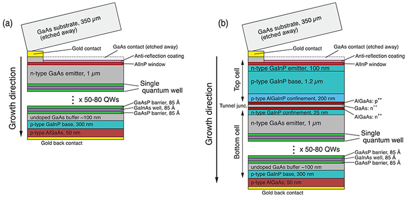
Quantum Wells Offer Possibilities
The inclusion of so many quantum wells in the bottom junction lowers that junction’s effective bandgap, increasing the wavelength of light it can absorb. Capturing longer wavelengths enables the tandem cell to nab more energy from the solar spectrum, making the cell more efficient at converting light to electricity.
Traditionally, quantum wells have primarily been used in lasers, LEDs, and electronics for telecommunications. As part of the development process, the NREL team produced a single-junction cell that demonstrated a very high external radiative efficiency (>40%)—the efficiency with which the cell converts electricity to light when run in reverse. While the team was not trying to build an LED device, their high-quality quantum wells demonstrated some potential in this area, too.
Strain Balancing Unlocks New Record
Previous work has attempted to use quantum wells to adjust the bandgap of solar cell junctions, but it has not produced any record-efficiency cells, in part because it is difficult to grow many, many layers of high-quality quantum well material. If the layers become too thick or the mechanical strain within the crystal lattice is not properly balanced, the cell develops defects.
For their world-record cell, the team alternated layers of gallium indium arsenide—in compression—and gallium arsenide phosphide—under tension. By carefully controlling the thickness of these layers, the strain of the compressive and tensile forces balances between layers. An array of lasers was used to measure the curvature of the wafer throughout the growth process, allowing the researchers to detect and adjust for strain in the crystal lattice.
“This work will lead to higher-efficiency solar cells for one-sun applications, which could be a significant driver of the widespread adoption of these cells,” said Myles Steiner, a senior scientist on the NREL team. “Now, a key challenge ahead is to learn how to manufacture these cells in a cost-competitive manner.”
Globe-Spanning Collaboration Yields Results
The development of this cell design grew out of a close collaboration between part of the High-Efficiency Crystalline Photovoltaics research group at NREL and a team at the University of New South Wales (UNSW). In fact, Steiner spent 3 months in early 2020 in New South Wales with his Australian collaborators, working on the project as part of a grant from the Fulbright Scholars Program.
“Our partnership brought together NREL’s long standing expertise in epitaxial growth and UNSW’s work in solar cell modeling, which helped us to collaborate effectively at a distance,” said Nicholas Ekins-Daukes, who led the UNSW team. “I was impressed with how quickly we were able to develop the first composite, strain-balanced semiconductor material to outperform a conventional solar cell.”
Learn more about photovoltaic research at NREL.
Last Updated Jan. 22, 2026