Reflectance Spectroscopy

In a fraction of a second, the photovoltaic (PV) reflectometer measures the reflectance spectrum of a wafer or cell that is dimensionally within 6 in. × 6 in.

The measured reflectance plots are deconvolved to derive physical parameters, including surface roughness and texture, antireflective coating thickness, metallization area and height, and backside metallization properties.

Pair of drawings showing how direct normal incident light reflects in a scatter from a rough surface and some scattered incident light to a spot reflects directly normal.

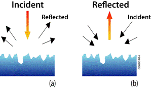
The reflectance measurement uses a principle of reciprocity

Schematic of the PV Reflectometer system; the Reflectometer itself at the left consists of a hollow sphere with light sources around the upper circumference, sample stage at the bottom and sensing equipment at the top; a diode array spectrometer at lower right and computer at upper right

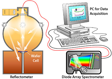
A schematic of the reflectometer

PV Reflectometer-generated graph of reflectance (Y-axis) versus wavelength (X-axis) for silicon PV wafers at three processing stages: texture-etched (highest reflectance), sawed and cleaned (slightly lower reflectance) and anti-reflection coated (significantly lower reflectance, with reflectance lowest for the coated stage in the 500 to 800 nanometer wavelength range.

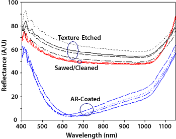
Reflectometer results on three groups of commercial PV-Si wafers (4.5 in. × 4.5 in.) at different stages of solar cell processing.
antireflective (AR) coating thickness: 794 to 858 Å

PV Reflectometer-generated graph of reflectance (Y-axis) versus wavelength (X-axis) for a different set of silicon PV wafers at four processing stages: after sawing (highest reflectance), after texturing (significantly lower reflectance), with conducting oxide coating (slight additionally lowered reflectance) and with anti-reflection coating (slight further lowered reflectance, more significant at the shorter wavelength range).

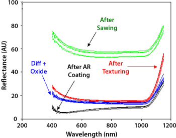
Reflectance curves (in arbitrary units) of 5-in. × 5-in. wafers taken with the PV-Reflectometer. These data yield information on the surface roughness, texture height, and oxide and AR coating thicknesses.
AR coating thickness: ˜600 Å

Andrew Ferguson

Group Manager, Spectroscopy And Photoscience

Andrew.Ferguson@nrel.gov
303-384-6637

Share