Quantum-Confined Semiconductors
NREL researchers seek to control the optical and electronic properties of quantum-confined semiconductors through doping.
This involves coupling of the core electronic structures to surface bound ligands or interactions with plasmonic nanoparticles to direct and transduce energy. We aim to utilize rational synthesis of nanocrystals, including production of asymmetric and multifunctional structures to investigate the unique phenomena offered by quantum confinement.
Controlling Exciton Recombination Using Polaritons
Controlling Exciton/Exciton Recombination in 2-D Perovskite Using Exciton–Polariton Coupling, Journal of Physical Chemistry Letters (2024)
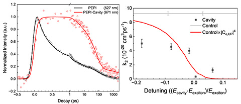
We demonstrate that exciton/exciton annihilation in the 2D perovskite (PEA)2PbI4 (PEPI)─ which defines the limiting efficiency in solar cells and light-emitting diodes, can be controlled through coupling of excitons to cavity polaritons.
Research Details
- Fabry-Pérot microcavities with varying thicknesses of the 2-D perovskite (PEA)2PbI4 (PEPI) were fabricated and studied using transient optical spectroscopy.
- Ultrafast spectroscopy showed an increase in recombination lifetime that could be modeled by a simple reduced interaction model owing to the increased photonic character in the coupled polariton states.
Significance and Impact
Control over the rate of exciton annihilation—a major loss mechanism in lasers, solar cells and other devices—could allow for much higher efficiency systems.
Partners
University of Colorado, Boulder
Past Research Highlights
Pickering Emulsions of Self-Assembled Lead Sulfide Quantum Dots With Janus-Ligand Shells as Nanoreactors for Photocatalytic Reactions, ACS Applied Nano Materials (2022)
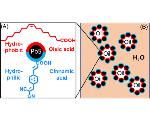
We prepared Pickering emulsions with semiconductor quantum dots (QDs). Amphiphilic lead sulfide (PbS) QDs are prepared by constructing Janus-ligand shells comprised of lipophilic oleic acid and hydrophilic 4- (2,2-dicyanovinyl)cinnamic acid ligands. Upon homogenizing, the QDs with Janus-ligand shells self-assemble at the water-dichloromethane interface forming stable Pickering emulsions.
Research Details
- PbS QD with Janus-ligand shells were fabricated.
- Pickering emulsions were characterized.
- Enhanced photocatalytic activity was measured.
Significance and Impact
Pickering emulsions have potential applications in a number of industries, e.g., biomedicine, food, catalysis, petroleum, and cosmetics, etc. QDs can endow Pickering emulsions with multiple interesting characteristics, such as strong photoluminescence, charge transfer to substrates in the different phases for photocatalytic reactions.
Partner
Size-Dependent Janus Ligand Shell Formation on PbS Quantum Dots, Journal of Physical Chemstry C (2021)
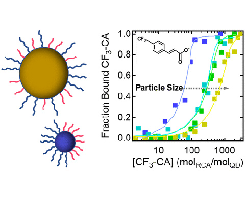
We found that Janus-ligand shells form more readily on smaller QDs than on bigger QDs likely because the ligand density is smaller on the larger QDs reducing the strength of the ligand-ligand coupling that drives Janus-ligand shell formation. This study broadens our understanding of how to construct Janus and patchy ligand shell morphologies on small QDs.
Research Details
- PbS QD with Janus-ligand shells were fabricated as function of size.
- 2D nuclear magnetic resonance was used the characterize the Janus-ligand shells.
Significance and Impact
Asymmetry is an essential property of any functional system. Janus nanoparticles (JNPs) are nanostructures that have an asymmetric distribution of one of its compositions, but yet still retain physically symmetric shape and have been intensely studied for a range of applications. Very few studies show how to form JNPs with semiconductor nanocrystals or QDs.
Partner
We discovered semiconducting molybdenum disulfide (MoS2) monolayers are heavily n-type doped or phase converted to the 1T/1T’ (metallic/semi-metallic) phase with n-butyl lithium immersion treatments. These doped or phase converted monolayers are stabilized by adding surface functional groups.
Research Details
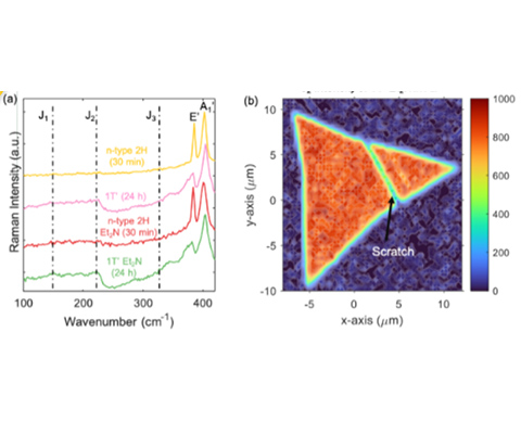
- Using n-butyl lithium treatments, we heavily n-type doped MoS2 monolayers with shorter immersion times (10–120 min) or convert MoS2 to the 1T/1T’ phase with longer immersion times (6–24 h).
- The n-butyl lithium treatments plus surface functionalization p-(CH3CH2)2NPh-MoS2 (Et2N-MoS2) maintain heavily n-type doped 2H phase or the 1T/1T’ phase across the monolayer for over 2 weeks.
- MoS2 monolayers are characterized with various confocal Raman, photoluminescence, absorption, X-ray photoelectron spectroscopy, scanning Kelvin probe microscopy, scanning electrochemical microscopy, and four-point probe sheet resistance measurements.
Significance and Impact
Transition metal dichalcogenide monolayers could be useful in a variety of applications, such as gas sensors, catalysis, field-effect transistors, etc. Our results provide a simple surface functionalization technique that will allow these monolayers to be incorporated into air-exposed devices.
Partners
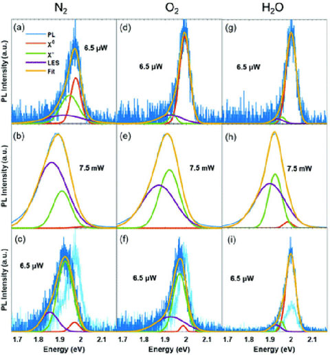
We have demonstrated the sensitivity of monolayer tungsten disulfide (WS2) to its local environment and its potential for detecting relative humidity.
Research Details
- Dry air (O2 in N2) plus illumination yields a photoluminescence increase and red shift that is due to increased trion emission, whereas humidified N2 (H2O vapor in N2) plus illumination results in an overall photoluminescence increase that is dominated by exciton emission.
- Time-resolved microwave conductivity shows both O2 or H2O vapor environment reduces WS2 photoconductivity, which is anti-correlated with the photoluminescence .
Significance and Impact
Monolayer WS2 is typically considered an inert 2D layer. However, we demonstrated that the optoelectronic properties are heavily influenced by the local environment. Therefore, this nanomaterial could be used as a relative humidity sensor via photoluminescence detection.
Partner
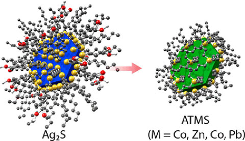
We developed a cation exchange reaction that produces a series of atomically thin (one monolayer) of metal sulfides. We specifically demonstrated atomically thin metal sulfides of PbS, CdS, ZnS, and Co2S.
Research Details
- Cation exchange reaction proceeds from monolayer Ag2S at room temperature.
- Optical properties suggest that the electronic structure of the atomically thin metal sulfides are unique.
Significance and Impact
The development of 2D or atomically thin material systems has led to the discovery of unique properties not found in bulk or 3D counterparts. Here we develop the synthesis of a new class of 2D semiconductors.
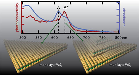
Measuring Photoexcited Free Charge Carriers in Mono- to Few-Layer Transition-Metal Dichalcogenides with Steady-State Microwave Conductivity, Journal of Physical Chemistry Letters (2020)
We used steady-state microwave conductivity for measuring charge generation action spectra in WS2 mono- to few-layer transition metal dichalcogenide systems at solar-equivalent light fluences. Multilayer portions of the sample were shown to be primarily responsible for the observed photoconductivity.
Research Details
- WS2 monolayers grown by chemical vapor deposition; increased sulfur produces more multi-layers
- Specially designed microwave cavity with exceptionally high sensitivity
- Complementary steady-state and time-resolved measurements for characterizing full mechanism
Significance and Impact
Multilayers are shown to be a primary source for the formation of long-lived free charges in transition metal dichalcogenides, an important finding for solar fuels and photovoltaics.
Steady-state microwave conductivity has the sensitivity to provide mechanistic information on charge carrier generation in mono- to few-layer semiconductors, where the total absorptance of light is less than 3%.
Partners
Contact
Share