Scanning Defect Mapping
Using optical scattering in the scanning defect mapping system (SDMS) produces a way to quickly identify and map defect distributions in silicon semiconductor wafers.
In this process, a wafer is first treated with an NREL-developed etch of hydrofluoric, acetic, and nitric acids to enhance the light scattered by the defects. The SDMS moves the treated wafer across a stationary laser beam and maps the defects for each location on the wafer. The amount of light reflected from an area is proportional to the dislocation density for that area and provides a direct statistical count of the number of dislocations.
Applications
Dislocation Mapping
Maps dislocation defects in silicon wafers quickly and accurately.
Grain Boundary Mapping
Maps grain boundaries in silicon wafers quickly and accurately.
PV Response Mapping
Compares photocurrent maps with the dislocation and grain-boundary maps to show the effect of defects and crystalline discontinuities on PV response.
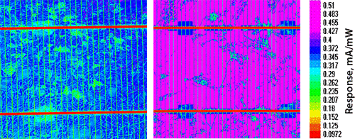
Laser beam induced current maps of two solar cells measured by PVSCAN, showing influence of defect-cluster density on the photoresponse.
Reflectance Mapping
Maps reflectance of the amount of light that does not penetrate the cell, called the completed cell. By mapping reflectance, the SDMS can calculate a cell's performance based on the light actually absorbed by the cell, which is a better measure of the effectiveness of the cell material.
Minority-Carrier Diffusion Length
Measures the average distance traveled by light-generated electrical carriers, which is the minority-carrier diffusion length in a completed solar cell.
Share